iC-TW29 26-BIT ENCODER PROCESSOR
WITH INTERPOLATION AND BiSS INTERFACE
Rev C1, Page 15/28
OPERATING REQUIREMENTS: BiSS Interface
Operating conditions: AVDD = DVDD = IOVDD = +3.1...+3.6 V, AVSS = DVSS = IOVSS = 0 V, Tj = –40...125 °C
Item Symbol Parameter Conditions Unit
No. Min. Max.
SSI protocol (BiSSEN pin high and BISS_CFG0.ssi = 1)
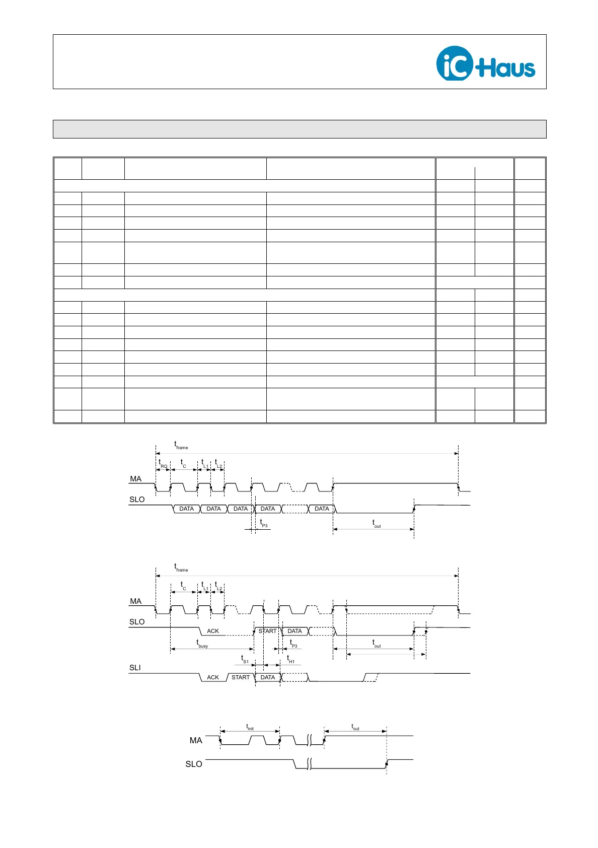
I201 t
frame
Permissible Frame Repetition * indenite
I202 t
C
Permissible Clock Period With t
RQ
according to I205 250 ns
I203 t
L1
Clock Signal Hi-Level Duration 125 t
out
ns
I204 t
L2
Clock Signal Lo-Level Duration 125 t
out
ns
I205 t
RQ
Request Time Clock low-level duration at MA input (due to
Elec. Char. 705)
500 ns
I206 t
P3
Output Propagation Delay 50 ns
I207 t
out
Slave Timeout see Elec. Char. 809
BiSS C protocol (BiSSEN pin high and BISS_CFG0.ssi = 0)
I208 t
frame
Permissible Frame Repetition * indenite
I209 t
C
Permissible Clock Period 100 ns
I210 t
L1
Clock Signal Hi-Level Duration 50 t
out
ns
I211 t
L2
Clock Signal Lo-Level Duration 50 t
out
ns
I212 t
busy
Processing Time 240 ns
I213 t
P3
Output Propagation Delay 50 ns
I214 t
out
Slave Timeout see Elec. Char. 809
I215 t
S1
Setup Time:
SLI stable before MA hi → lo
25 ns
I216 t
H1
Hold Time: SLI stable after MA hi → lo 10 ns
Note: * Allow t
out
to elapse.
t
P3
DATA
t
C
DATA
t
out
t
frame
t
L2
t
RQ
DATADATADATA
MA
SLO
t
L1
Figure 9: SSI protocol timing
MA
SLO
t
C
DATA
t
frame
t
L2
t
L1
ACK
t
busy
t
out
t
P3
START
START DATAACK
SLI
t
S1
t
H1
Figure 10: BiSS protocol timing
Figure 11: BiSS slave timeout