iC-TW29 26-BIT ENCODER PROCESSOR
WITH INTERPOLATION AND BiSS INTERFACE
Rev C1, Page 10/28
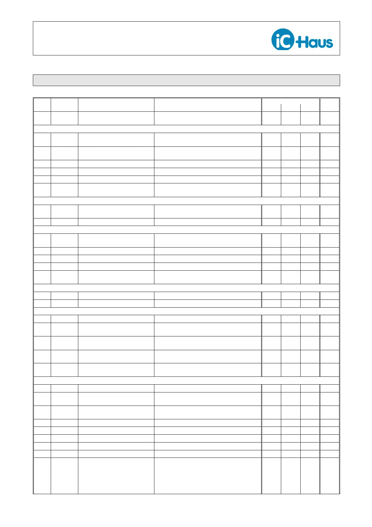
ELECTRICAL CHARACTERISTICS
Operating conditions: AVDD = DVDD = IOVDD = 3.1...3.6 V, Tj = –40...+125 °C, reference point AVSS unless otherwise stated
Item Symbol Parameter Conditions Unit
No. Min. Typ. Max.
206
Rin()diff Differential Input Resistance
MAIN_CFG.zero = 0 10 1000 MΩ
MAIN_CFG.zero = 1 0.620 MΩ
Converter Performance
304 INL
Integral Nonlinearity (over one
input SIN/COS cycle)
Refer to Figure 5, 1 Vpp-diff SIN/COS input
with compensated offset, gain and phase
0.2 °
305 DNL
Differential Nonlinearity (over one
input SIN/COS cycle
Refer to Figure 5, 1 Vpp-diff SIN/COS input
with compensated offset, gain and phase
0.1 °
307 t
AB
Output Phase A vs. B Refer to Figure 4 25 %
308 t
whi
Duty Cycle at Output A, B Refer to Figure 4 50 %
309 AArel Relative Angle Accuracy Refer to Figure 4, at conditions of 305 2 %
310 t
MTD
Time Between AB Edges
(Minimum Transition Distance)
Refer to Figure 4, ABLIMIT = 0 1/fosc 20 ns
Internal Oscillator
401
fosc Oscillator Frequency
Tj = 27 °C; AVDD, DVDD = 3.1 V 48 51 MHz
AVDD, DVDD = 3.6 V 48 52 MHz
402 TCf Temperature Coefcient 225 ppm/K
Internal EEPROM
501 Nwrite
Permissible Number of Write
Cycles
Tj = –40 °C...85 °C 1000
502 Tjw Write Temperature Range –40 85 °C
503 Tjr Read Temperature Range –40 125 °C
504 DRTraw Raw Data Retention Time 10 years
505 DRTact
Actual Data Retention Time (with
error correction)
Tj = 85 °C 50 years
Reset and Start-Up: xRST
601 DVDDonoff DVDD Power-On/Off Threshold xRST tied to DVDD 2.5 2.7 3.0 V
603 tstart Startup Time Valid EEPROM conguration, START.wait = 0 2 ms
Digital Input Pins: xRST, xCALIB, A+/– (Encoder Link active), A– and B– (BiSS mode), SI, SCLK, xSS,GPIO, BISSEN
701 Vt()hi Input Logic Threshold High DVDD = 3.6 V 1.9 V
702
Vt()lo Input Logic Threshold Low
DVDD = 3.3 V 0.8 V
703 Ilk() Input Leakage Current at
SI, SCLK, xSS
±50 nA
704
f(SCLK) Permissible SPI Clock Frequency
at SCLK
TEST.spi = 0 20 MHz
TEST.spi = 1 40 MHz
705
t
RQ
Request Time at MA (A+)
BiSSEN = high; for SSI data output to SLO, 24 / fosc
see Figure 9
Digital Output Pins: xIRQ, SO, A+/A–, B+/B–, Z+/Z– (CMOS drivers enabled: MAIN_CFG.rs422 = 0), Z– (BiSS mode)
801 I()max Permissible Output Current Per pin, indenite ±10 mA
802
Vout()hi Output Voltage High
I() = –4 mA, 2.4 V
MAIN_CFG.irqpp = 1 (for xIRQ push-pull)
803
Vs()hi Saturation Voltage High
Vs()hi = IOVDD - V(); I() = -4 mA, 0.7 V
MAIN_CFG.irqpp = 1 (for xIRQ push-pull)
804 Vs()lo Saturation Voltage Low I() = 4 mA 0.7 V
805 Isc()hi Short-Circuit Current High Any pin shorted to DVSS –30 –16 mA
806 Isc()lo Short-Circuit Current Low Any pin shorted to DVDD 16 30 mA
807 tr() Rise Time DVDD = 3.3 V, CL = 50 pF, 10% → 90% VDD 20 ns
808 tf() Fall Time DVDD = 3.3 V, CL = 50 pF, 10% → 90% VDD 20 ns
809
t
out
() Slave Timeout at SLO (B+)
BiSSEN = high; for BiSS & SSI, see Figure 11;
BiSS_CFG0.at = 0 (xed) 1024
/ fosc
BiSS_CFG0.at = 1 (adaptive) 8 / fosc t
init
+ 1024
4 / fosc / fosc