iC-TW29 26-BIT ENCODER PROCESSOR
WITH INTERPOLATION AND BiSS INTERFACE
Rev C1, Page 16/28
OPERATING REQUIREMENTS: ADI Interface
Operating conditions: AVDD = DVDD = IOVDD = +3.1...+3.6 V, AVSS = DVSS = IOVSS = 0 V, Tj = –40...125 °C
Item Symbol Parameter Conditions Unit
No. Min. Max.
BiSS Protocol (ADI_CFG.biss = 1)
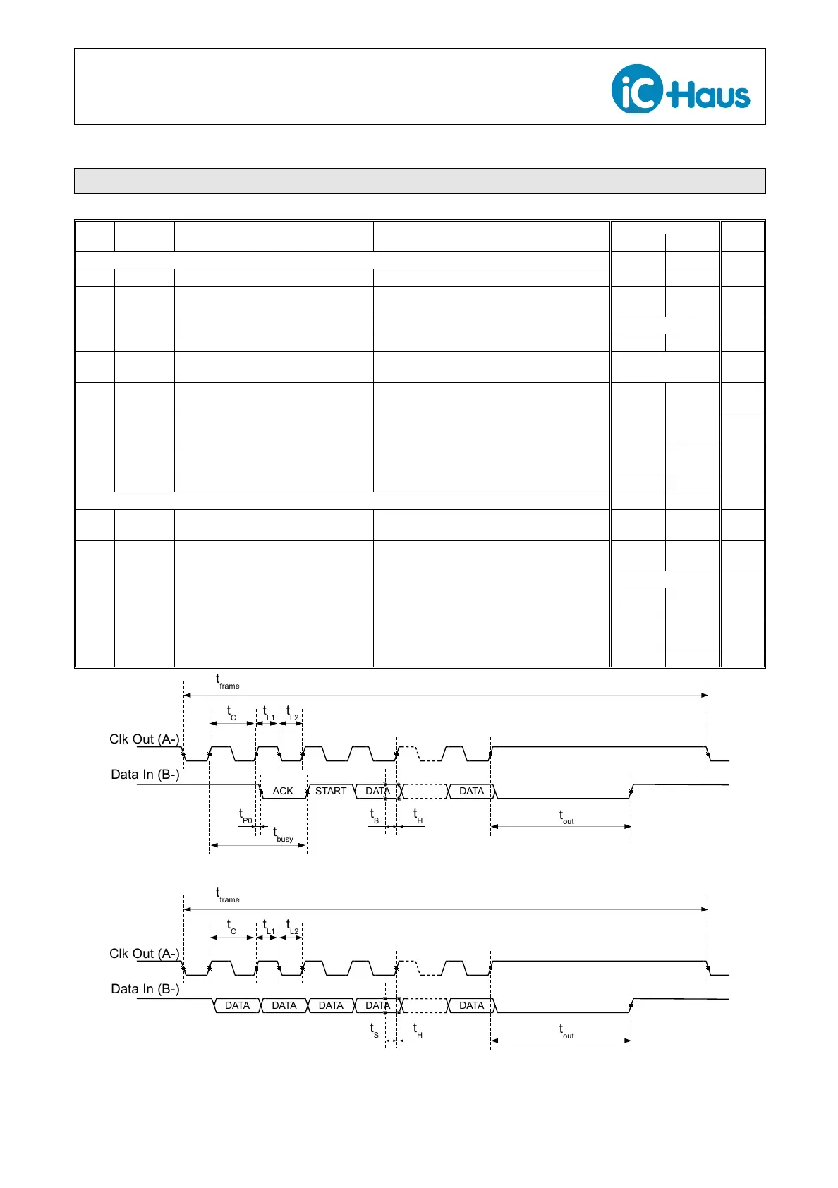
I301 t
frame
Clock Frame Repetition Note: This value can vary during operation. 1 3 ms
I302 t
C
Clock Period
ADI_CFG.freq = 0 5.9 7.7 µs
ADI_CFG.freq = 1 0.59 0.77 µs
I303 t
L1
, t
L2
Clock Signal Hi/Lo Level Duration 50 % t
C
I304 t
busy
Permissible Processing Time relative to clock period ∞ % t
C
I305 t
P0
Permissible Propagation Delay
(Line Delay Compensation)
not supported
(data is captured on next rising clock edge)
0 ns
I306 ∆t
P
Permissible Propagation Delay
Variance
not supported (refer to t
S
and t
H
) % t
C
I307 t
S
Setup Time:
Data stable before clock edge lo → hi
without line delay compensation (t
P0
= 0) 100 ns
I308 t
H
Hold Time:
Data stable after clock edge lo → hi
without line delay compensation (t
P0
= 0) 0 ns
I309 t
out
Permissible Slave Timeout t
C
µs
SSI Protocol (ADI_CFG.biss = 0)
I310 t
frame
Clock Frame Repetition Note: This value can vary unpredictably during
operation.
1 3 ms
I311 t
C
Clock Period
ADI_CFG.freq = 0 5.9 7.7 µs
ADI_CFG.freq = 1 0.59 0.77 µs
I312 t
L1
, t
L2
Clock Signal Hi/Lo Level Duration 50 % t
C
I313 t
S
Setup Time:
Data stable before clock edge lo → hi
100 ns
I314 t
H
Hold Time:
Data stable after clock edge lo → hi
0 ns
I315 t
out
Permissible Slave Timeout t
C
µs
Clk Out (A-)
Data In (B-)
t
H
START DATA
t
C
t
S
DATA
t
out
t
frame
t
L2
t
L1
ACK
t
busy
t
P0
Figure 12: ADI timing with BiSS protocol
t
H
DATA
t
C
t
S
DATA
t
out
t
frame
t
L2
t
L1
DATADATADATA
Clk Out (A-)
Data In (B-)
Figure 13: ADI timing with SSI protocol