iC-TW29 26-BIT ENCODER PROCESSOR
WITH INTERPOLATION AND BiSS INTERFACE
Rev C1, Page 4/28
PACKAGING INFORMATION (Compatible with iC-TW28)
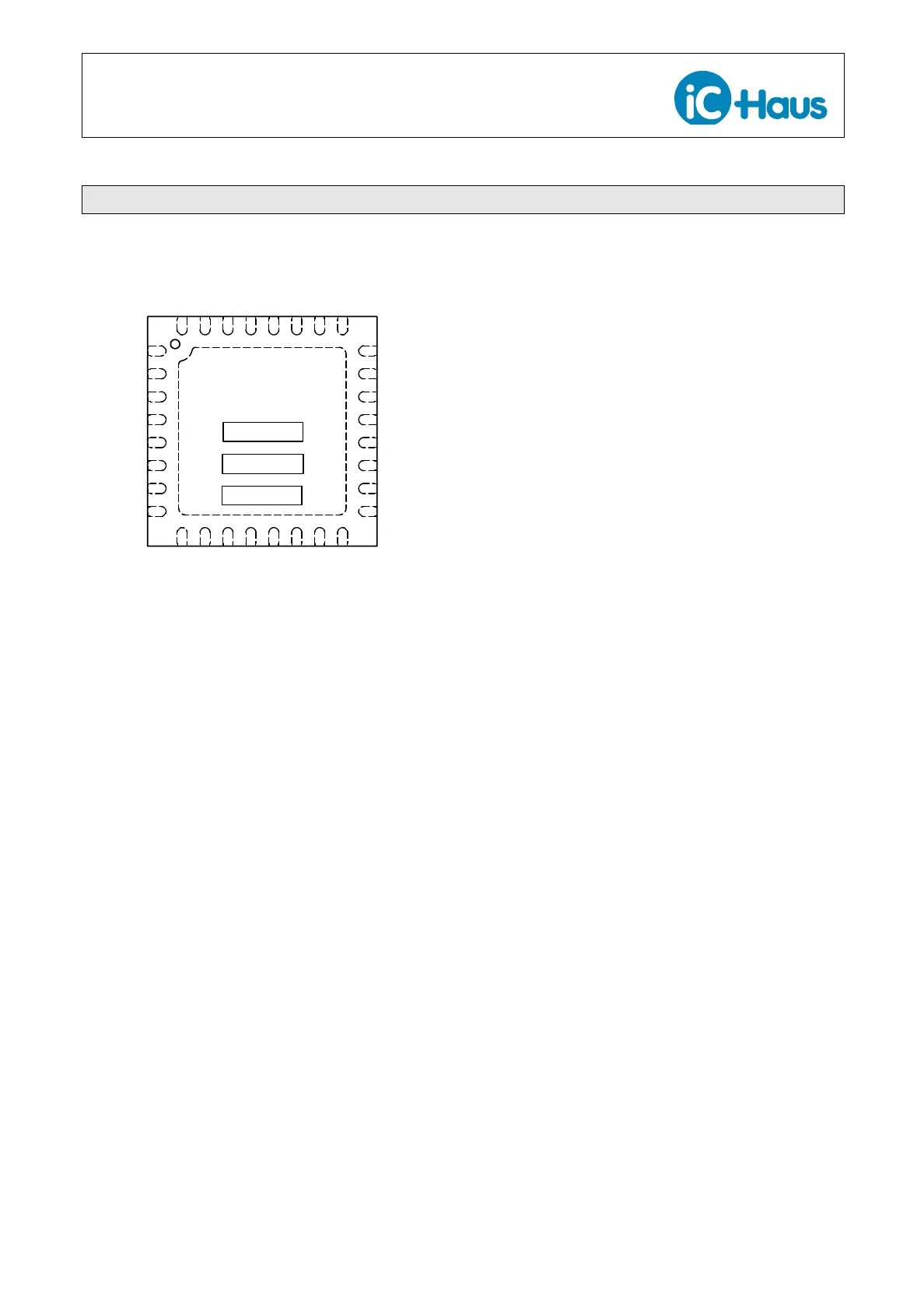
PIN CONFIGURATION QFN32-5x5
1
2
3
4
5
6
7
8
9
10
11
12 13
14
15
16
17
18
19
20
21
22
23
24
252627282930
31
32
<D-CODE>
<A-CODE>
<P-CODE>
PIN FUNCTIONS
No. Name Function
1 SIN+
3
+ Differential Sine Input
2 SIN–
3
– Differential Sine Input
3 AVDD +3.3 V Analog Power Supply Input
4 COS+
3
+ Differential Cosine Input
5 COS–
3
– Differential Cosine Input
6 AVSS Analog Ground
7 ZERO+
4
+ Differential Zero (Index) Input
8 ZERO–
4
– Differential Zero (Index) Input
9 VREF ADC Reference Voltage Output
10 VC Bias Output (VDD/2)
11 Reserved
1
Must be connected to ground
12 Reserved
1
Must be connected to ground
13 GPIO
3
General Purpose I/O
14 xRST
4
Reset Input (low active)
15 xCALIB
4
Auto-Calibration Input (low active)
16 xIRQ
4
Interrupt Request (active-low)
Input/Output or Fault Output
17 Z– – Differential RS422 Z Output
or Multifunction I/O
18 Z+ + Differential RS422 Z Output
or Multifunction I/O
19 IOVSS I/O Ground
20 B– – Differential RS422 B Output
or Multifunction I/O
21 B+ + Differential RS422 B Output
or Multifunction Output
22 IOVDD +3.3 V I/O Power Supply Input
23 A– – Differential RS422 A Output
or Multifunction I/O
24 A+ + Differential RS422 A Output
or Multifunction I/O
25 DVDD +3.3 V Digital Power Supply Input
26 LED
4
LED Intensity Control Output
or General-Purpose I/O
27 DVSS Digital Ground
28 SO SPI Slave Output (Master Input)
29 SI
3
SPI Slave Input (Master Output)
30 SCLK
3
SPI Clock Input
31 xSS
4
SPI Slave Select Input
32 BISSEN
5
BiSS Interface Enable
TP
2
Backside paddle
IC top marking: <P-CODE> = product code, <A-CODE> = assembly code (subject to changes), <D-CODE> = date code (subject to changes);
1
Must be connected to ground.
2
Must be connected to a ground plane at AVSS potential. Can also be used to connect DVSS.
3
Do not allow to oat. Connect to ground via 10 kΩ resistor if not used.
4
Do not allow to oat. Connect to 3.3 V or ground via 10 kΩ resistor if not in use. Alternatively, program MAIN_CFG.zero = 1 for internal biasing.
5
Connect to 3.3 V (to DVDD for to enable BiSS interface) or ground (to DVSS to disable BiSS interface). Do not allow to oat.