3-1
SECTION 3 CIRCUIT DESCRIPTION
• PA AND TUNER UNITS (Receive circuits)
• PA AND TUNER UNITS (Transmit circuits)
ATT
PRE
AMP
Q1211
Q1212/Q1213
LPF
LPF A
HPF A
PHASEI
PHASE
DET
SWR
DET
SWRL
ATT
IMPI
D961,D962
PWR/SWR
DET
MUTE
LPF
RL801
From the TX circuits
MUTE
BPF
BPF
BPF
BPF
BPF
BPF
BPF
BPF
LPF
BPF
BPF
BPF
BPF
TPWRLBUFF
D1505
IMP
DET
D1271
TUNE
NET
TUNER UNIT
IC1701
HF/50 MHz/70 MHz
D1311 D1312
PA UNIT
fc=76 MHz
Q811
D811/D812
IC1701
To the TX AMP
D1081~D1083
D1001
50.00-54.00 MHz
22.00-29.99 MHz
30.00-49.99 MHz
54.01-69.99 MHz
70.00-74.80 MHz
15.00-21.99 MHz
2.00-2.99 MHz
4.50-6.49 MHz
10.00-14.99 MHz
3.00-4.49 MHz
1.60-1.99 MHz
8.00-9.99 MHz
6.50-7.99 MHz
1.60-30.00 MHz
POWER
DET
D1201
IC1901
D/A
IC1331
D/A
PIN
D1251
D1231
ATT
AF
AMP
AF
AMP
A/D
AMP BUFF
LPF
AAF
AF
AMP
RF
Q746
L731,L732
C731~C735
SW
SP1
J101
J1302
1
2
3
4
5
6
7
8
9
10
11
12
13
D/A
IC902
FLASH
MEMORY
LPF
LVDS
DRIVE
IC1212
BPF
XTAL
AMP
IC1221
MAIN
DSP
CPU
IC901
HSK0/HSK1/DRESD/FRWT
IC301
MAIN UNIT
RF UNIT
DSPCK/DSPR/FRM/BCLK
FPGA
IC1351
41.344 MHz
(41.344 MHz)
Q1202
Q1201
DACLK
X1201
IC1211
IC721
IC992
IC992
SCPCK/SCPR/SCPX/SCPSS
5.BAND
10.FSKK
3.HSEND
13.SQLS
4.START
7.NC
11.MOD
1.8V
2.GND
9.KEY
6.ALC
[ACC]
12.AF
8.14V
FPDX/FPSR/FPSX
[EXT-SP]
[SP]
DR_AF/DR_RSV/DX_REC/DX_FMT
IC991
D/A
AGCV
IC971
124.033 MHz
/FPCAL/BCLK/FRM/MCLK
FPX_AGC/FPX_DET/FPR_MOD
SPCS/SPCK/
SPDO/SPDI
AFO
J1
1
2
3
4
5
6
7
8
J1
DISPLAY UNIT
FRONT UNIT
GND
MIC U/D
MIC
+8V
SQL
PTT
MICE
PHONE UNIT
MIC UNIT
AF OUT
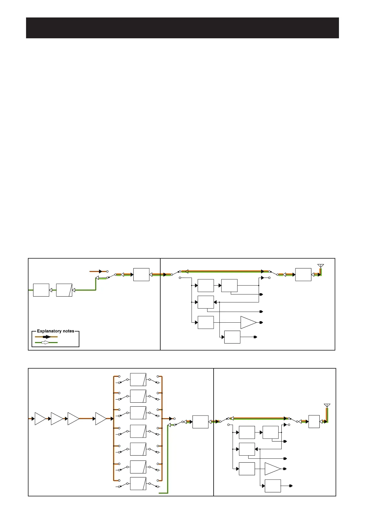
3-1 PA UNIT
The PA UNIT is composed of the transmit power amplifier,
harmonic filters, and sensing circuits for the transmit power
and SWR.
(1) RECEIVE SIGNAL PROCESSING
The received signal from the TUNER UNIT is passed through
the TX/RX SW (RL801), and applied to the RF UNIT through
the LPF whose cut-off frequency is 76 MHz, and the TX mute
switch (Q811, D811 and D812).
To prevent abnormal oscillations caused by feedback of the
transmit signal, the TX mute switch connects the transmit line
to ground while receiving.
(2) TRANSMIT SIGNAL PROCESSING
• DRIVE AMPLIFIER
The transmit signal from the RF UNIT is sequentially ampli-
fied by the RF amplifier (Q101), pre-drive amplifier (Q111)
and drive amplifier (Q121). These RF amplifiers are the high
gain source-grounded amplifiers. The idling current of drive
amplifier (Q121) is appropriately adjusted to compensate for
variation in gain.
• POWER AMPLIFIER
The transmit signal from the drive amplifier (Q121) is applied
to the push-pull power amplifier (Q131 and Q132) to be ampli-
fied up to 100 watts (for the HF/50 MHz band) or 50 watts (for
the 70 MHz band).
The idling current of the power amplifier
is appropriately adjusted to compensate for variation in gain.
• LPF
The transmit signal from the power amplifier is filtered by
one of the LPFs that is selected according to the transmit
frequency. These LPFs are the Chebyshev filters with sharp
cut-off characteristics, to reduce the harmonic components in
the transmit signal.
There are 7 BPFs with different cut-off frequencies. The LPFs
are selected by the relays on both sides of each LPF, accord-
ing the transmit frequency.
•
FORWARD AND REFLECT WAVES DETECTION CIRCUIT
The transmit signal is passed through the SWR detection cir-
cuit, which is composed of the CM coupler and rectifier diodes
(D961 and D962). The forward and reflect waves are detected,
resulting in the forward wave and reflect wave sensing volt-
ages. The sensing voltages are amplified by the buffer (IC981),
and then applied to the CPU in the MAIN UNIT for monitoring.
The amplified transmit signal is applied to the antenna,
through the TUNER UNIT.
PRE
AMP
Q1411
LPF
YGR
AMP
IC1031
RF
LPF
LPF
DRIVE
AMP
LPF
PWR
AMP
Q131
Q132
LPF
DRIVE
PRE
LPF
LPF
LPF
RF
AMP
D961,D962
PWR/SWR
DET
PIN
D1021
ATT
PIN
D1041
ATT
HPF
ATT
ALC
ALC
RL801
To the RX circuit
BPF
BPF
BPF
BPF
BPF
BPF
BPF
BPF
LPF
BPF
BPF
BPF
BPF
0.03-1.59 MHz
14.35-21.45 MHz
0.03-2.0 MHz
2.0-4.0 MHz
PA UNIT
21.45-33.0 MHz
33.0-76 MHz
Q111
7.3-14.35 MHz
Q121
4.0-7.3 MHz
Q101
1.60-74.80 MHz
D1051
D1052
22.00-29.99 MHz
50.00-54.00 MHz(TX)
30.00-49.99 MHz
54.01-69.99 MHz
70.00-72.00 MHz(TX)
15.00-21.99 MHz
2.00-2.99 MHz
4.50-6.49 MHz
10.00-14.99 MHz
3.00-4.49 MHz
8.00-9.99 MHz
6.50-7.99 MHz
1.60-30.00 MHz
AMOD
A/D
MIC
AMP
LPF
MICI
A/D
IC1001
RF UNIT
IC1003
IC1002
IC1002
D/A
IC1331
L1281,L1282
C1281,C1283,C1285
PIN
D1251
D1232
ATT
A/D
AMP BUFF
RF
J1302
1
2
3
4
5
6
7
8
9
10
11
12
13
LPF
LVDS
DRIVE
IC1212
BPF
XTAL
AMP
IC1221
MAIN UNIT
FPGA
IC1351
41.344 MHz
(41.344 MHz)
Q1202
Q1201
DACLK
X1201
IC1211
5.BAND
10.FSKK
3.HSEND
13.SQLS
4.START
7.NC
11.MOD
1.8V
2.GND
9.KEY
6.ALC
[ACC]
12.AF
8.14V
124.032 MHz
/FPCAL/BCLK/FRM/MCLK
FPX_AGC/FPX_DET/FPR_MOD
J1
1
2
3
4
5
6
7
8
DISPLAY UNIT
GND
MIC U/D
MIC
+8V
SQL
PTT
MICE
MIC UNIT
AF OUT
PHASEI
PHASE
DET
SWR
DET
SWRL
ATT
IMPI
SW11
SW11
TPWRL
BUFF
D1505
IMP
DET
D1271
TUNE
NET
TUNER UNIT
IC1701
HF/
50 MHz/
70 MHz
D1311 D1312
IC1701
POWER
DET
D1201
IC1901
TX signal
RX signal

 Loading...