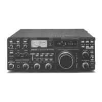
•VCO CIRCUIT
•
LOOP
SYSTEM
11
-4
LOGIC CIRCUITS
(1)
CPU INPUT CONTROL
(2)
DISPLAY CIRCUIT
The
performance
of
the
VCO
is very
important
for
PLL
operation.
In order
to obtain
a high
carrier-to-noise
(C/N)
ratio
and
a
stable
oscillator
output, four
separate
VCOs
are
used.
Each
is
assigned a
quarter of the
total
necessary
bandwidth.
The power supply
for the
VCOs
is
doubly
regulated
when
compared
with the reference
frequency
oscillator.
Furthermore,
coreless
coils
are used for the
oscillator
coils
in
order
to
obtain
a
high
Q
as
well
as immunity from
external
induction.
The
output
of the
VCO
is
separated
into
two
parts after
passing
through
the
Q22
buffer
amplifier.
One
part
is
amplified
by
023,
and after impedance
matching
by
025,
is
output
to the RF
unit
as the
1st
LO.
The
output level
is
about
0dBm/50ohms.
The
other part
is
fed
back
to
the
PLL
loop
through
the
026 buffer
amplifier.
The
VCO signal is
then mixed
”With
the
in-loop
LO
by IC3
to be
down-mixed. The
output
from
the
mixer
is
passed through
the
bandpass
filter
with
a
bandwidth of
about
40
to 70MHz
to
eliminate
the
spurious
components.
The output
is then amplified
by the 016
and 017 cascade
amplifier, and
input
to IC2
to
form the PLL.
The
functions of this
unit
include the
control
of frequency, the
processing
of
BPF, LPF
and mode signals,
the output of
data
for the
PLL unit and display
unit, etc.
This unit
includes an 8-bit NMOS
CPU,
a
4-bit Ik
word
CMOS RAM,
a
multi-purpose
custom
1C
and
I/O
expander IC's.
CIRCUIT
A
multi-function CMOS 1C is used. This custom
1C is contained in
a
40-pin OIL package.
(a)
An
external L and C are connected to pins
18
and 19
to
give an
approximate
clock signal
of 100kHz.
(b) ATS
from pin 32 is HIGH
if
the TUNING CONTROL Is rotated
faster
than
a set
speed. The
set
speed
is
fixed by the values of
C6
and R7 connected to pin
21
(TC).
The
high
level
is
used
as
a
strobe
signal which switches the dial-pitch (tuning rate) of
the
matrix input.
(c)
Ml
and M2
at
pins
38
and
37
are used
to switch the multiplic-
tion
factors of
the input pulses from the TUNING
CONTROL.
200
pulses per
one rotation are obtained by
50
pulses
x 4. For
RIT/zdTX control, the multiplication factor is
two
times to
give
50
pulses
X
2
=
100
pulses
per one rotation.
The
luminescent display
tube
(DS1)
is
driven
by
the IC1 and IC2
drivers.
These ICs contain
such functions as
input data
latches,
clock oscillators,
timing counters,
segment
decoders, etc.
The
clock
frequency
is set by C2
and C6.
Displays
for
the
RIT/zlTX shift
frequency
and
memory
channel are
driven by IC2,
and other
displays are
driven
by
IC1.
The
signals
for
the
display
of "RTTY"
through
"GENE" are sent
from the
LOGIC
unit
to
each segment.
The segments
are
switched
by
the digit signals, TO to
T6 from
IC1 and T3
from IC2,
and lit
dynamically. The
letters "RIT",
"ziTX",
and
"DUP" are
con-
nected to the
same digit
in the
tube, thus
the necessary
word is
selected by T4,
T1 and TO
digit signals
and
dynamically lit.
-
52
-