CIRCUIT DESCRIPTION
LPF
ANT
SW
BPF
RF
AMP
BPF
BPF
BPF
D131
D92
D52
From the TX AMP circuit
To the 1st IF circuit
Q90
D93
D130
RF UNIT
X170
450KHz
BPF
X1
21.25MHz
From the 1st IF circuit
IC1
PLL IC
IF IC
REF
IC170
FI170
450KHz
2ND LO
DET
To the RX AF circuit
RF UNIT
SP1
SP
AF
AMP
AMP
D/A
IC190
VOLIN
VOL
From the demodulator circuit
LPF
AF
MUTE
DE-
ENPHA
IC363C
IC260D
IC362
IC363A
AF
SW
NOISE CANCEL IC
IC382
IC380
MIC signal
MAIN UNIT
BPF
IF
AMP
21.7MHz
FI150
Q151
From RF AMP
To the IF IC
1st LO signal
from the VCO
Q150
FI151
RF UNIT
4-1 RECEIVE CIRCUITS
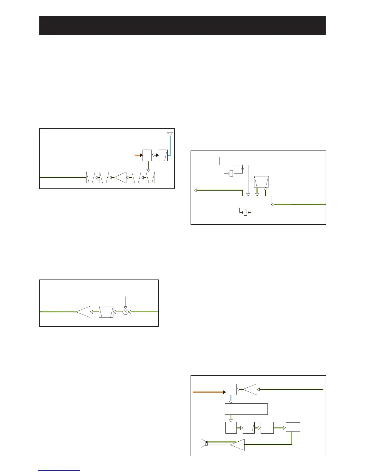
RF CIRCUIT (RF UNIT)
The RX signal from the antenna is passed through a two-
staged LPF (L81, L82, C83–C86 and C89), ANT SW (D90),
and two tuned BPFs (D92, D93, L92, L93, C95, C97–C100
and C117), and then applied to the RF AMP (Q90).
The amplifi ed signal is applied to the 1st IF circuit, through
two tuned BPFs (D130, D131, L96, L97, C109, C110 and
C112–C115).
1ST IF CIRCUIT (RF UNIT)
The RX signal from the RF circuits is applied to the 1st IF
mixer (Q150), and mixed with the 1st LO signal from the VCO
(Q21, Q22, and D20–D22), resulting in a 21.7 MHz 1st IF
signal.
The 1st IF signal is fi ltered by the 1st IF fi lters (FI150 and
FI151), and then applied to the 1st IF AMP (Q151). The am-
plifi ed signal is applied to the 2nd IF circuits.
2ND IF CIRCUIT (RF UNIT)
The 1st IF signal from the 1st IF circuits is applied to the IF IC
(IC170, pin 16). The IF IC contains the 2nd IF mixer, 2nd IF
AMP, detector, and so on, in its package.
The 1st IF signal is mixed with the 21.25 MHz 2nd LO signal
from the reference frequency oscillator (TCXO: X1), resulting
in a 450 kHz 2nd IF signal. The 2nd IF signal is passed through
the 2nd IF fi lter (FI170) to remove sideband noise. The fi ltered
signal is amplifi ed by the 2nd IF AMP, and demodulated by
the quadrature detector with discriminator (X170).
The demodulated AF signal is applied to the RX AF circuits
on the MAIN UNIT.
RX AF CIRCUIT (MAIN UNIT)
The demodulated AF signal from the IF IC (RF UNIT: IC170)
is amplifi ed by the AF AMP (IC363A), and then applied to
the noise canceller IC (IC382, pin 36), through the AF SW
(IC380, pins 7, 1).
The processed AF signal is passed through the AF mute SW
(IC260D, pins 11, 10), LPF (IC363C, pins 9, 8) and de-em-
phasis circuit (R279 and C266), and then applied to the D/A
converter (IC190, pin 1) to adjust the level.
The level-adjusted AF signal is amplifi ed by the AF AMP
(IC362), and then output to the internal speaker (CHASSIS:
SP1).
When an external speaker is connected, the AF signal from
the D/A converter (IC190, pin 2) is amplifi ed by the AF AMP
(IC362), and then output to the external speaker, through
J290.
 Loading...