4 - 8
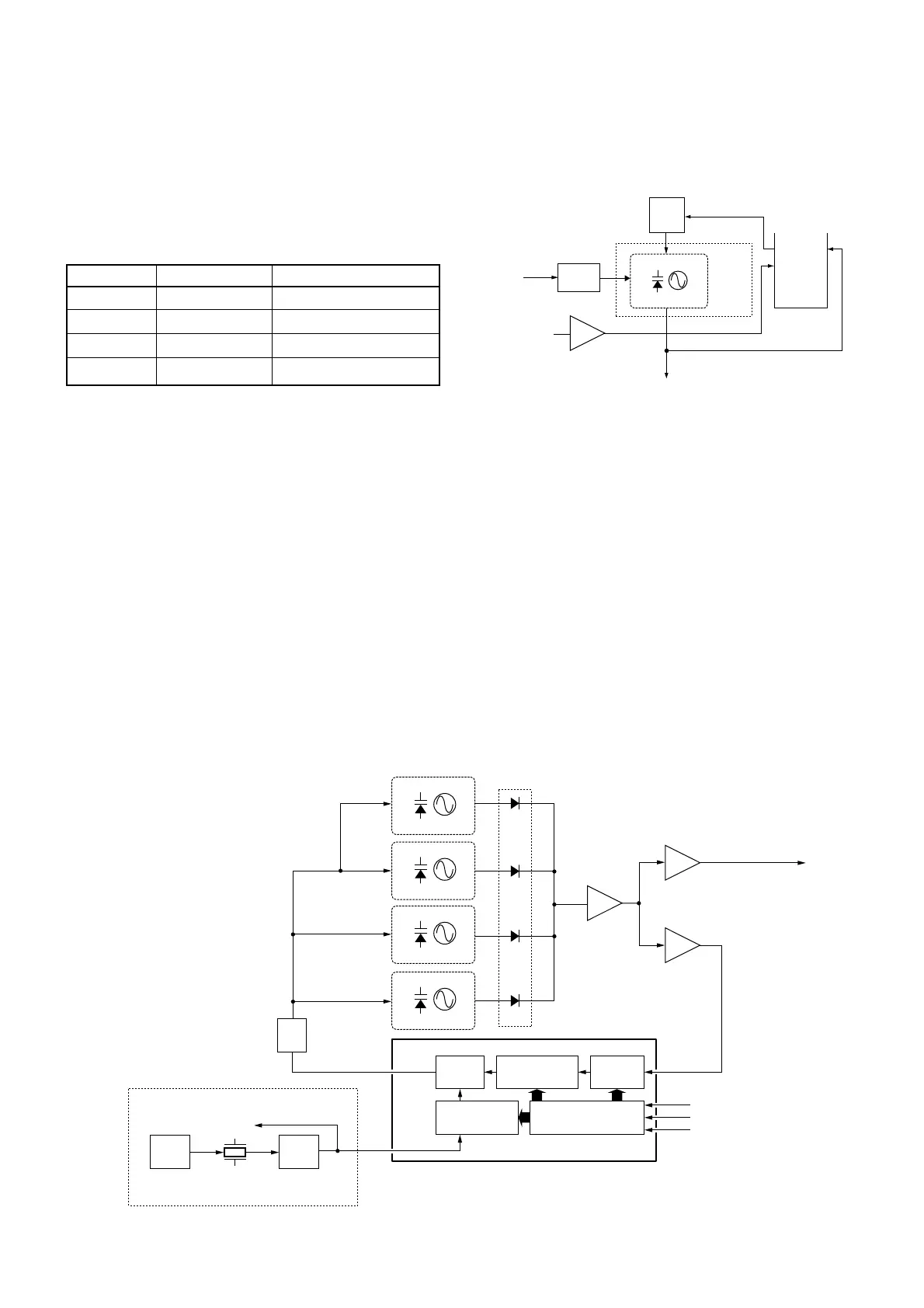
A portion of the signal from the buffer amplifier (IC2) is
amplified at the buffer amplifier (Q8) and is then fed back to
the PLL IC (IC3, pin 11) as the comparison signal.
• B-BAND CIRCUIT (1STBVCO BOARD)
The oscillated signal at 1st B-VCO circuits is applied to the
buffer amplifiers (IC2) via one of the LO switches (D7–D10).
The amplified signal is applied to the 1st mixer circuit (RF
unit; IC15, pin 3) via the LO amplifier (Q9). Components and
osillating frequences of each circuits are as follow list.
A portion of the signal from the buffer amplifier (IC2) is
amplified at the buffer amplifier (Q8) and is then fed back to
the PLL IC (IC3, pin 11) as the comparison signal.
4-2-4 2ND VCO CIRCUITS
(2NDCVCO AND 2NDDVCO BOARDS)
The 2nd VCO circuit generates the 2nd LO frequencies, and
the signals are applied to the 2nd mixer circuit.
• A-BAND CIRCUIT (2NDCVCO BOARD)
The 2nd C-VCO circuit (Q1 and D1) generates 409.4500
MHz and 448.7500 MHz. The oscillated signal is applied to
the 2nd mixer (RF unit; IC10, pin 3), and is then mixed with
the 1st IF signal.
A part of oscillated signal from the 2nd C-VCO circuit is
applied to the PLL IC (IC1, pin 8) as the comparison signal,
and is then output from pin 5. The signal passes through the
loop filter (R14, R15 and R22), and is then applied to the 2nd
C-VCO circuit again as PLL lock voltage.
• 2ND C VCO CIRCUIT
1st B-VCO Components Oscillating freq. (MHz)
1BVCO Q1, D1 and D2 863.3–1099.6999
2BVCO Q2 and D3 683.3–866.6999
3BVCO Q3 and D4 566.3–686.6999
4BVCO Q4, Q5 and D5 384.7–441.6999
 Loading...