4.4.4 RECORDING SPEECH CIRCUIT (LOGIC UNIT)
When the STOP signal from the MAIN UNIT is applied
to
IC3(A), the
output
of
IC3(A) becomes
"LOW"
for
approximately 1 sec. from the rise
of
the STOP signal.
When the
[RECORDER-SPEECH] SWITCH
is
ON,
after
1 sec. from the rise
of
the STOP signal (if the
VSC
signal
is
"HIGH"),
05
and
04
are
switched
on, and
the
SPKS signal
is
output.
5V
D7
EQ4C
C13
STOP~------+----.----~
>'--H---.--.....---spKs
~
N
a:
Fig.12
5V
l!RECORDER-SPEECHJ
OFF
: o<J
I
I
I
L
___
_
I
DB~
[VSC)
OFF
4.4.5 SCAN SPEED CONTROL CIRCUIT (LOGIC UNIT)
This
circuit
accelerates the speed
of
the MEMORY
CHANNEL SCAN, SELECTED MODE SCAN and
SELECTED MEMORY SCAN.
By the PRIO signal, the
output
of
IC16 remains
"HIGH"
even while receiving the another frequency.
When
021 is switched
ON
by a PRIO
or
a
PRO
signal,
C7
is
input in parallel
with
CS,
and the
clock
fre-
quency will decrease.
5V
LOGIC
UNIT!
[SCAN-SPEED)
064
Fig.13
4·4·6
81
- 84, BH, BS AND
VS
SIGNALS
co:
ct::
isw2
UNIT
,....
~-----------
ii:
The LOGIC UNIT supplies
following
signals
with
the
PLL
UNIT and
RF
UNIT.
RECEIVE
FREQUENCY
SIGNALS
FRX
[MHz]
B1
B2 B3 B4
BH
BS
vs
25-
89.9999
H L L
1025-1089.9999
L H
90-
249.9999
L H
L
L L
1090-1249.999~
- -
250-
511.9999
L L H H L
1250-1511.9999
512-
761.9999
L L
L L
H
1512-1761.9999
H
-
H
-
762-
999.9999
L L
L
H L
1762-1999.9999
B1-B4,
BH: BPF signals
BS: Band signal
VS: VCO selector signlal
Table 10
4-10
4·5 DISPLAY CIRCUIT (DISPLAY
UNln
This
circuit
is
consists
of
a fluorescent display tube
DS1,
display tube drivers IC1, IC2 and a DC-DC con-
verter circuit.
4·5·1
FREQUENCY DISPLAY CIRCUIT
IC1
drives the
display
of
frequencies while IC2 drives
the display
of
memory channels.
Signals from the LOGIC UNIT and the MAIN UNIT
control
IC1
and IC2.
4·5·2
MODE DISPLAY CIRCUIT
IC2 allocates
T3-T7
for five types
of
data, and IC2
send the segment
data
"1"
to
R19.
EXAMPLE:
The AND
circuit
of
"Q
" and
"T7''
is configured
with
R18
and
R19.
05
and
010
are switched
ON
by the
timing
of
"T7"
only
when
"Q"
is at
"HIGH",
and
then the letter
"SCAN"
lights
up.
5V
T7
R19
Fig. 14
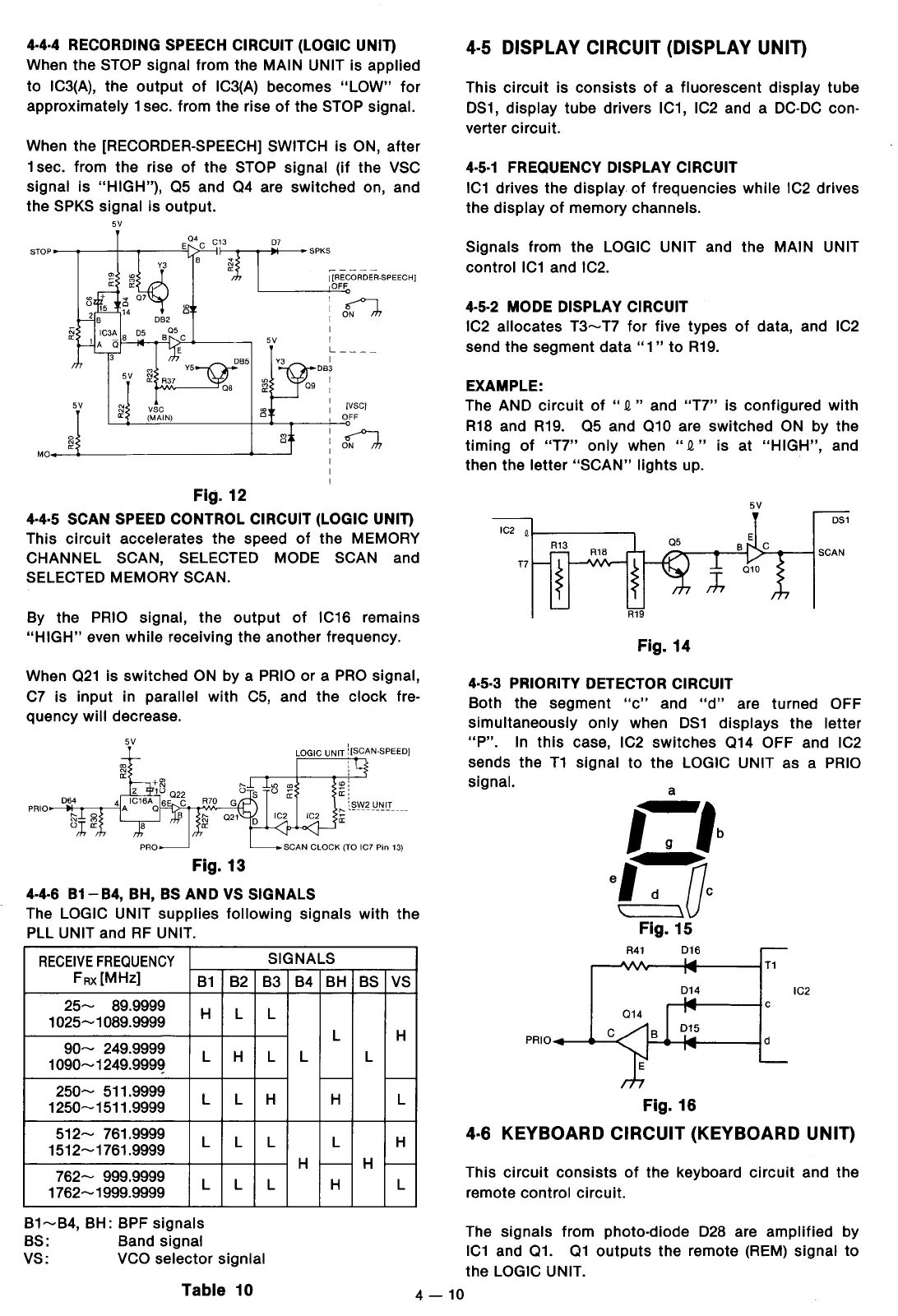
4.5.3 PRIORITY DETECTOR CIRCUIT
Both the segment
"c"
and
"d"
are turned OFF
simultaneously
only
when
DS1
displays the letter
"P".
In
this
case, IC2
switches
014
OFF and IC2
sends the
T1
signal
to
the LOGIC UNIT as a PRIO
signal.
a
I
g
1·
ef
d
v,
'
\
Fig.15
R41
016
T1
014
IC2
c
PRIO
c
d
Fig. 16
4·6 KEYBOARD CIRCUIT (KEYBOARD UNIT)
This
circuit
consists
of
the keyboard
circuit
and the
remote control circuit.
The signals from photo-diode
D28
are
amplified
by
IC1
and
01.
01
outputs
the remote (REM) signal
to
the LOGIC UNIT.
 Loading...