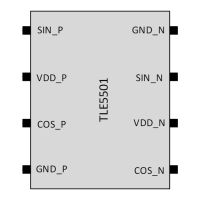
2 Serial Inspection and Configuration Interface (SICI)
The sensor features a digital 16bit bidirectional one wire interface (SICI). Connect the A
OUT
pin to a GPIO port in
order to establish a communication between the sensor and the controller.
2.1 Hardware Implementation
Figure 4 SICI application circuit
To activate the interface the AOUT shall be forced to GND during and after the sensor startup.
The communication is based on transmitting a bit stream to the sensor driven by an external controller. For this
interface, the A
OUT
pin is used as an I/O pin to read from the device and to write the registers of the device by
driving the pin with a defined timing.
The interface timing specification is shown in Table 1 and described in Figure 6 and Figure 7.
2.2 Entering Communication Mode
After or while suppling the sensor, the A
OUT
pin shall be forced to GND to enter the interface mode of the device.
Figure 5 shows the “interface enable time” t
IFen
which is the valid time window to enable the SICI interface. This
low state has only to be present once after start up to allow the device to receive the 16 bit enter-interface-
command. The activation will also work if the A
OUT
stays at ground from the beginning. While sending the enter-
interface-command, the device answers to each sent bit with logic “0” as shown in Figure 5.
After sending the enter-interface-command, the A
OUT
pin will remain at V
Sens
(open drain). If the interface
activation is not successful the A
OUT
pin will reflect the quiescent voltage.
To enable the access to the sensor memory the internal intelligent state machine (ISM) needs to be disabled with
a dedicated command like described in chapter 3.
 Loading...