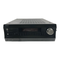
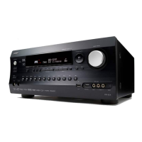
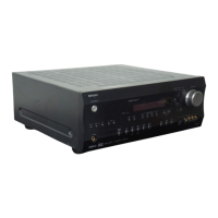
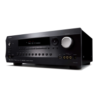
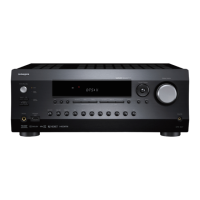
DTR-4.6
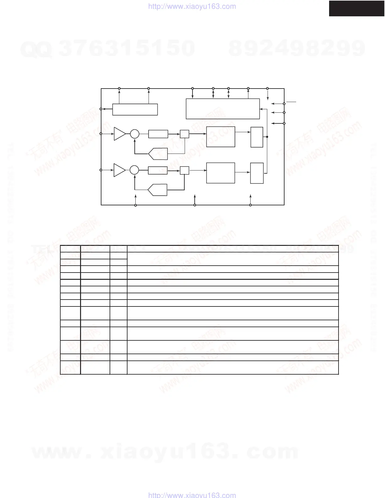
IC BLOCK DIAGRAMS AND DESCRIPTIONS
VQ REFGND
FILT+
AINL
Voltage Reference
AINR
S/H
S/H
DAC
LP Filter
LP Filter
DAC
Q
Q
V
L
1.8V-5.0V SCLK LRCK SDOUT MCLK
Serial Output Interface
RST
M0
M1
High
Pass
Filter
High
Pass
Filter
Digital
Decimation
Filter
Digital
Decimation
Filter
VD
3.3V-5.0V
GND
VA
3.3V-5.0V
+
+
-
-
CS5340-CZZ(101dB,192kHz, Multi-Bit Audio A/D Converter)
Pin Pin Name I/O Descri
tion
1M0 I
16 M1 I
2 MCLK I Master Clock-Clock source for the delta-si
ma modulator and di
ital filters.
3VL Lo
ic Power-Positive
ower su
l
for di
ital in
ut/out
ut.
4 SDOUT O Serial Audio Data Out
ut-Out
ut for two's com
lement serial audio data.
5,14 GND Ground-Connect to the analo
round.
6VD IDi
ital Power-Positive
ower su
l
for the di
ital section.
7 SCLK I/O Serial Clock-Serial clock for the serial audio interface.
Left Right Clock-Determines which channel, Left and Right, is currently
active on the serial audio data line.
9 RST I Reset-The device enters a low
ower mode when low.
10 AINL I
Analog Input-The full scale analog input level is 0.56Vp-p.
12 AINR I
Quiescent Voltage-Filter connection for the internal quiescent
reference voltage.
13 VA Analo
Power-Positive
ower su
l
for the analo
section.
Positive Voltage Reference-Positive reference voltage for the internal
sampling circuits.
15 FILT+ O
Mode Selection-Determines the operational mode of the device.
8 LRCK I/O
11 VQ O
w
w
w
.
x
i
a
o
y
u
1
6
3
.
c
o
m
Q
Q
3
7
6
3
1
5
1
5
0
9
9
2
8
9
4
2
9
8
T
E
L
1
3
9
4
2
2
9
6
5
1
3
9
9
2
8
9
4
2
9
8
0
5
1
5
1
3
6
7
3
Q
Q
TEL 13942296513 QQ 376315150 892498299
TEL 13942296513 QQ 376315150 892498299
http://www.xiaoyu163.com
http://www.xiaoyu163.com
 Loading...