DTR-4.6
IC BLOCK DIAGRAMS AND DESCRIPTIONS
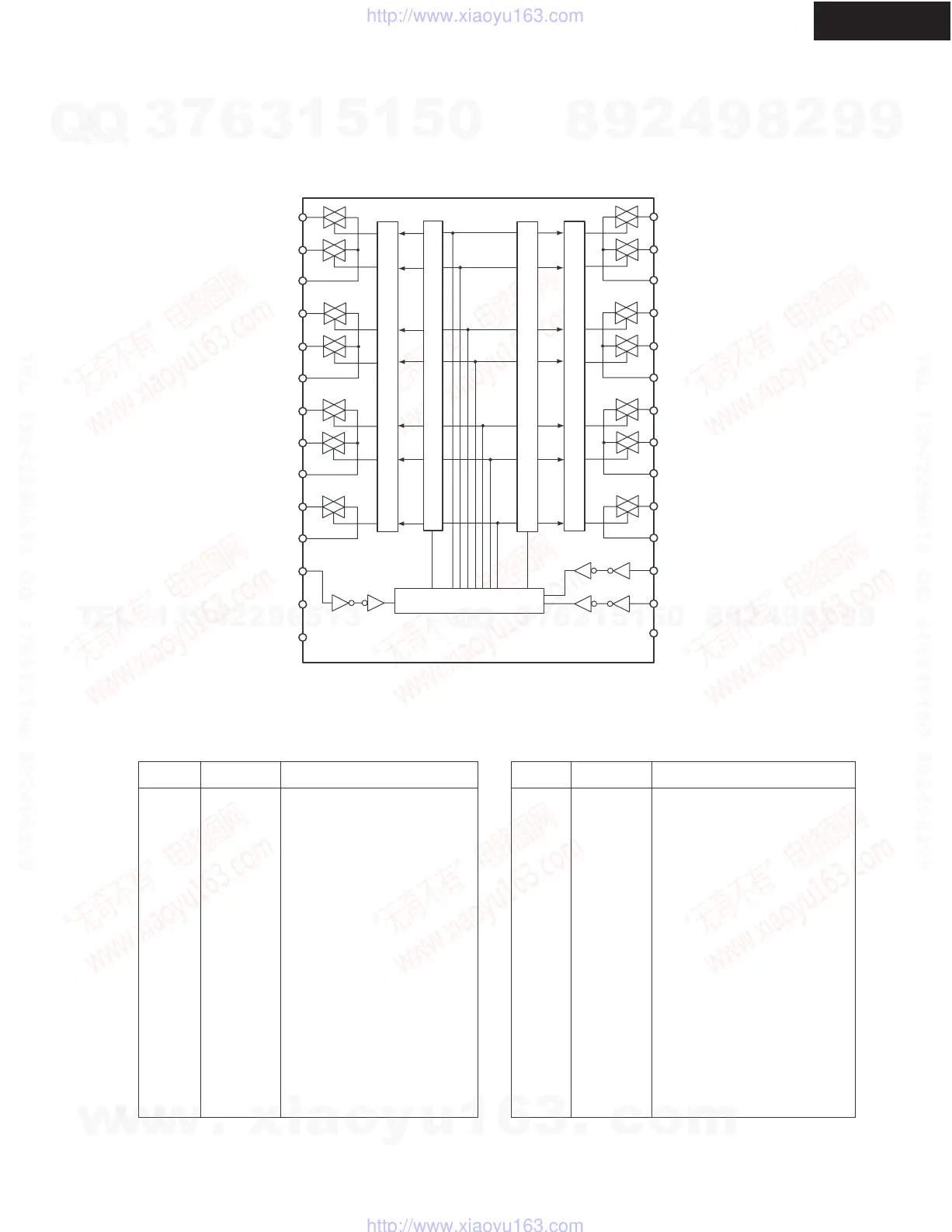
NJU7311AM (Analog Function Switch)
BLOCK DIAGRAM
TERMINAL DESCRIPTION
L1
L2
L-COM1
L3
L4
L-COM2
L5
L6
L-COM3
L7
L-COM4
ST
R1
R-COM1
R2
R3
R4
R-COM2
R5
R6
R-COM3
R7
R-COM4
CK
DATA
VSS
VDD
VEE
Latch Circuit
Level Shifter
Control Circuit
Latch Circuit
Level Shifter
1
2
3
4
5
6
7
8
9
10
11
12
13
14
15
16
17
18
19
20
21
22
23
24
25
26
27
28
VEE
L1
L2
L-COM1
L3
L4
L-COM2
L5
L6
L-COM3
L7
L-COM4
ST
VSS
CK
DATA
R-COM4
R7
R-COM3
R6
R5
R-COM2
R4
R3
R-COM1
R2
R1
VDD
Pin No. Pin Name Description
Pin No. Pin Name Description
Negative Voltage Supply
Analog switch input/output
Analog switch input/output
L1, L2, Common
Analog switch input/output
Analog switch input/output
L3, L4 common
Analog switch input/output
Analog switch input/output
L5, L6 Common
Analog switch input/output
L7 Common
Chip enable
GND
Clock input
Data input
R7 Common
Analog switch input/output
R5, R6 Common
Analog switch input/output
Analog switch input/output
R3, R4 Common
Analog switch input/output
Analog switch input/output
R1, R2, Common
Analog switch input/output
Analog switch input/output
Positive voltage supply
w
w
w
.
x
i
a
o
y
u
1
6
3
.
c
o
m
Q
Q
3
7
6
3
1
5
1
5
0
9
9
2
8
9
4
2
9
8
T
E
L
1
3
9
4
2
2
9
6
5
1
3
9
9
2
8
9
4
2
9
8
0
5
1
5
1
3
6
7
3
Q
Q
TEL 13942296513 QQ 376315150 892498299
TEL 13942296513 QQ 376315150 892498299
http://www.xiaoyu163.com
http://www.xiaoyu163.com
 Loading...