IC BLOCK DIAGRAMS AND TERMINAL DESCRIPTIONS -87
TERMINAL DESCRIPTION
TX-NR905/NA905
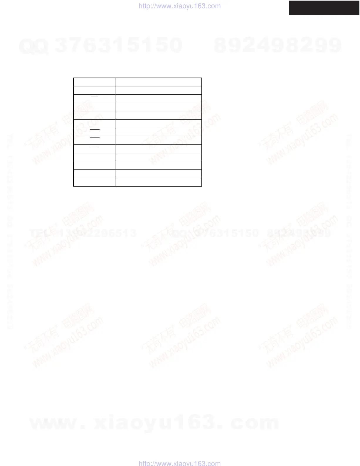
Q213, Q214: K4M563233G (256 Mbit SDRAM)
Pin Name Pin Function
CLK System Clock
CS
Chip Select
CKE Clock Enable
A
0 ~ A11 Address
BA
0 ~ BA1 Bank Select Address
RAS
Row Address Strobe
CAS Column Address Strobe
WE Write Enable
DQM
0 ~ DQM3 Data Input/Output Mask
DQ
0 ~ 31 Data Input/Output
V
DD/VSS Power Supply/Ground
V
DDQ/VSSQ Data Output Power/Ground
w
w
w
.
x
i
a
o
y
u
1
6
3
.
c
o
m
Q
Q
3
7
6
3
1
5
1
5
0
9
9
2
8
9
4
2
9
8
T
E
L
1
3
9
4
2
2
9
6
5
1
3
9
9
2
8
9
4
2
9
8
0
5
1
5
1
3
6
7
3
Q
Q
TEL 13942296513 QQ 376315150 892498299
TEL 13942296513 QQ 376315150 892498299
http://www.xiaoyu163.com
http://www.xiaoyu163.com


 To Next Page