Datasheet 27
Electrical Specifications
Notes:
1. Unless otherwise noted, all specifications in this table apply to all processor frequencies.
2. V
IL
is defined as the maximum voltage level at a receiving agent that will be interpreted as a logical low
value.
3. V
IH
is defined as the minimum voltage level at a receiving agent that will be interpreted as a logical high
value.
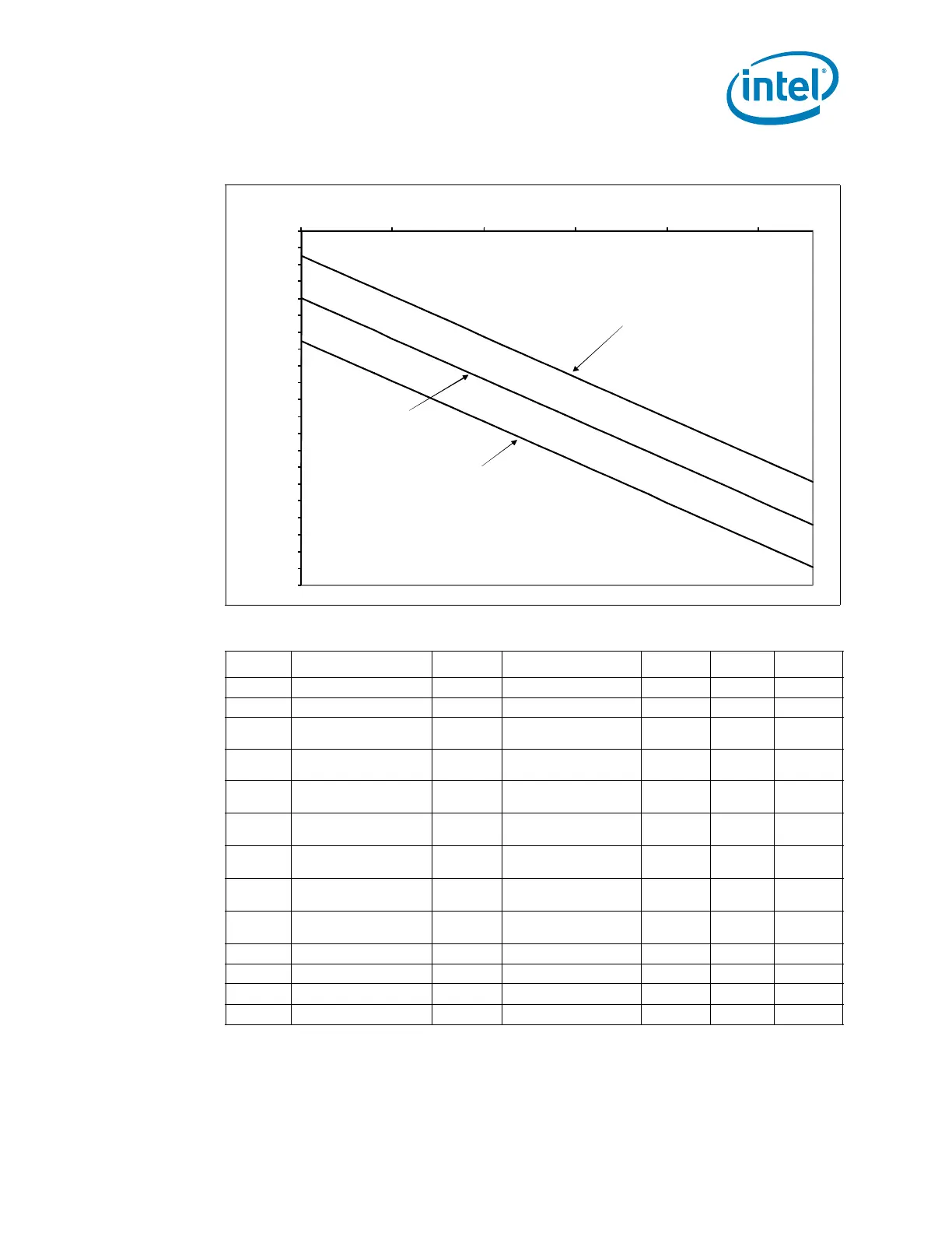
Figure 2-4. V
TT
Static and Transient Tolerance Load Line
Table 2-11. DDR3 Signal Group DC Specifications
Symbol Parameter Min Typ Max Units Notes
1
V
IL
Input Low Voltage — 0.43*V
DDQ
V2,4
V
IH
Input High Voltage 0.57*V
DDQ
——V3
V
OL
Output Low Voltage
—
(V
DDQ
/ 2)* (R
ON
/
(R
ON
+R
VTT_TERM
))
—V
V
OH
Output High Voltage
—
V
DDQ
– ((V
DDQ
/ 2)*
(R
ON
/(R
ON
+R
VTT_TERM
))
—V4
R
ON
DDR3 Clock Buffer On
Resistance
21 — 31 Ω
R
ON
DDR3 Command Buffer
On Resistance
16 — 24 Ω
R
ON
DDR3 Reset Buffer On
Resistance
25 — 75 Ω
R
ON
DDR3 Control Buffer On
Resistance
21 — 31 Ω
R
ON
DDR3 Data Buffer On
Resistance
21 — 31 Ω
I
LI
Input Leakage Current N/A N/A ± 1 mA
DDR_COMP0
COMP Resistance 99 100 101 Ω 5
DDR_COMP1
COMP Resistance 24.65 24.9 25.15 Ω 5
DDR_COMP2
COMP Resistance 128.7 130 131.30 Ω 5
-0.2125
-0.2000
-0.1875
-0.1750
-0.1625
-0.1500
-0.1375
-0.1250
-0.1125
-0.1000
-0.0875
-0.0750
-0.0625
-0.0500
-0.0375
-0.0250
-0.0125
0.0000
0.0125
0.0250
0.0375
0.0500
0 5 10 15 20 25
V
t
t
V
Itt [A] (sum of Itta and Ittd)
Vtt Maximum
Vtt Typical
Vtt Minimum
 Loading...