CIRCUIT DESCRIPTION
5-13
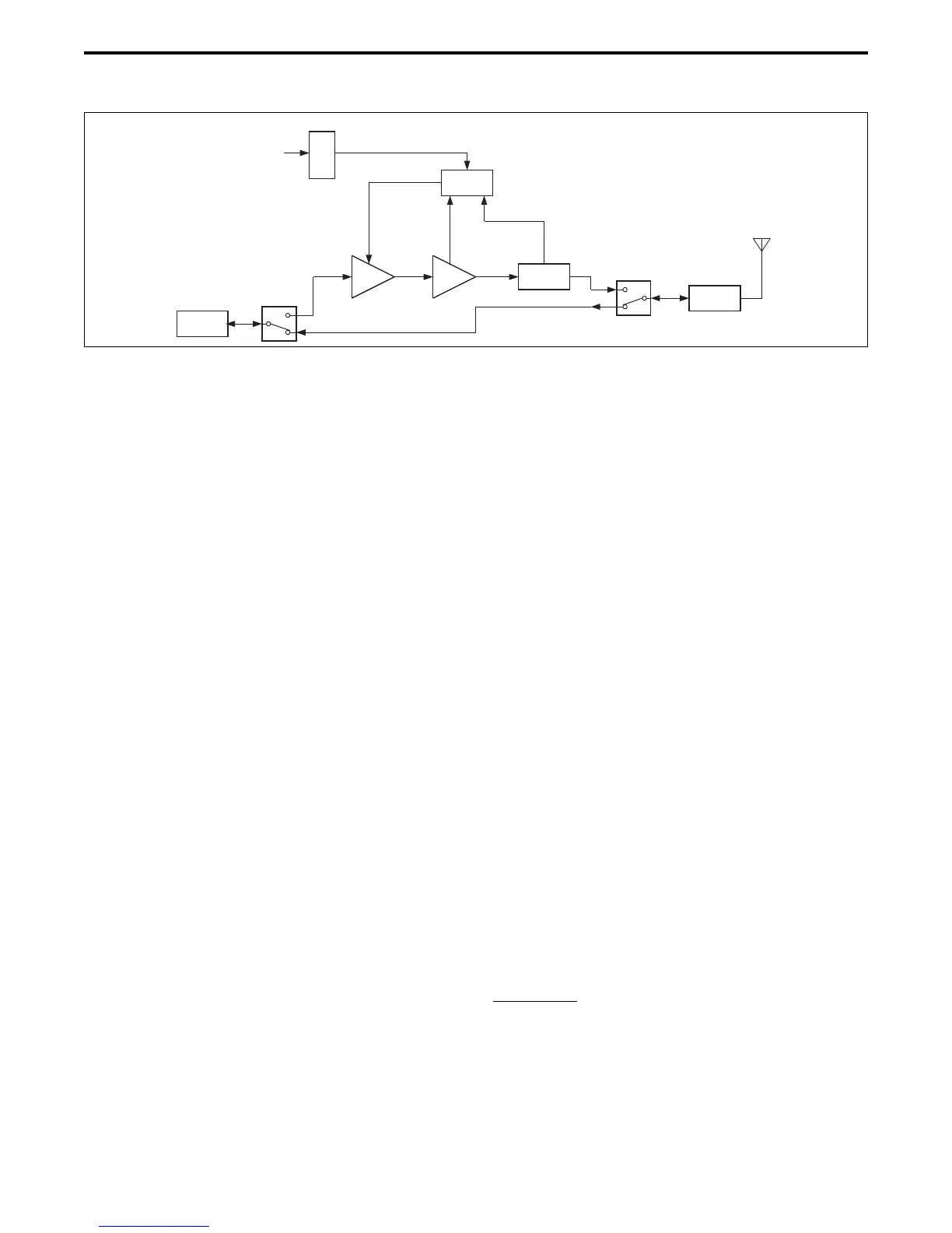
Figure 5-3 VHF 50W PA Board Block Diagram
RF Board
Low Power
Antenna Sw
Driver
Q509
Final Amp
Q510
Low-Pass
Filter
High Power
Antenna Sw
Power
Sense
Antenna
Current
Sense
Power
Control
U501
Shift Register
Power Adjust
From Logic Bd
then has a low impedance path through C533 and
CR513 to driver Q509, and the high impedance
provided by CR512 blocks it from the receive path.
In the receive mode, the opposite occurs, so
CR513 is reverse biased and CR512 forward biased.
The receive signal from the high power antenna switch
(see following) then has a low impedance path through
C544, CR512, and C534 to the RF board, and is
blocked from the power amplifier by CR513.
The high power antenna switch consists of pin
diodes* CR501, CR502, and CR503. This switch
effectively switches the antenna between the power
amplifier and the receive bypass path to the RF board
(see preceding illustration).
Transistor Q501 is on in the transmit mode and
off in the receive mode. Therefore, in the transmit
mode, all three diodes are forward biased (CR501 and
CR502 are biased by voltage applied from the
collector of Q510). The transmit signal then has a low
impedance path through CR502 to the low-pass filter
and is blocked from the bypass path by L504/C511
and L505/C515 which present a high impedance at the
transmit frequency. In the receive mode, all three
diodes are reverse biased. Therefore, the receive signal
from the antenna is blocked from the power amplifier
by CR502 and has a low impedance path through
L504 and L505 to the RF board.
5.6.2 AMPLIFIERS (Q509, Q510)
Impedance matching between the low power
antenna switch and Q509 is provided by L511 and
several capacitors and sections of microstrip. Class C
biasing is provided by L510 and ferrite bead EP503,
and negative feedback for stabilization is provided by
R557 and R543. Supply voltage to Q509 is controlled
by the power control circuit to regulate the power
output of the transmitter. Conditioning and isolation of
the DC supply to Q509 is provided by L509, L514,
EP501, and C540-C542.
Impedance matching between Q509 and final
amplifier Q510 is provided by several capacitors and
sections of microstrip. Class C biasing of Q510 is
provided by L515, EP502, R559, and R560. The
current for this stage flows through L516, R561, and
L517. The voltage drop across R561 is sensed by the
power control circuit to detect an over-current
condition.
From Q510 the transmit signal is fed through
another impedance matching network to a directional
coupler, to the high power antenna switch (see
preceding section), and then to the low-pass filter. This
filter attenuates harmonics occurring above the
transmit frequency band to prevent adjacent channel
interference. The directional coupler detects the
forward component of the output power for use by the
power control circuit.
5.6.3 POWER CONTROL
Introduction
The power control circuit maintains a constant
power output as changes occur in temperature and
voltage. It does this by sensing forward power and
then varying the drive to Q510 to maintain a constant
output power. The drive to Q510 is controlled by
* A reverse biased pin diode presents a high impedance to RF signals.
Conversely, and a forward biased pin diode presents a variable low
impedance that changes inversely to current.
VHF 50W PA BOARD (CONT’D)
 Loading...