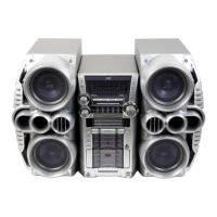
HX-Z1
45
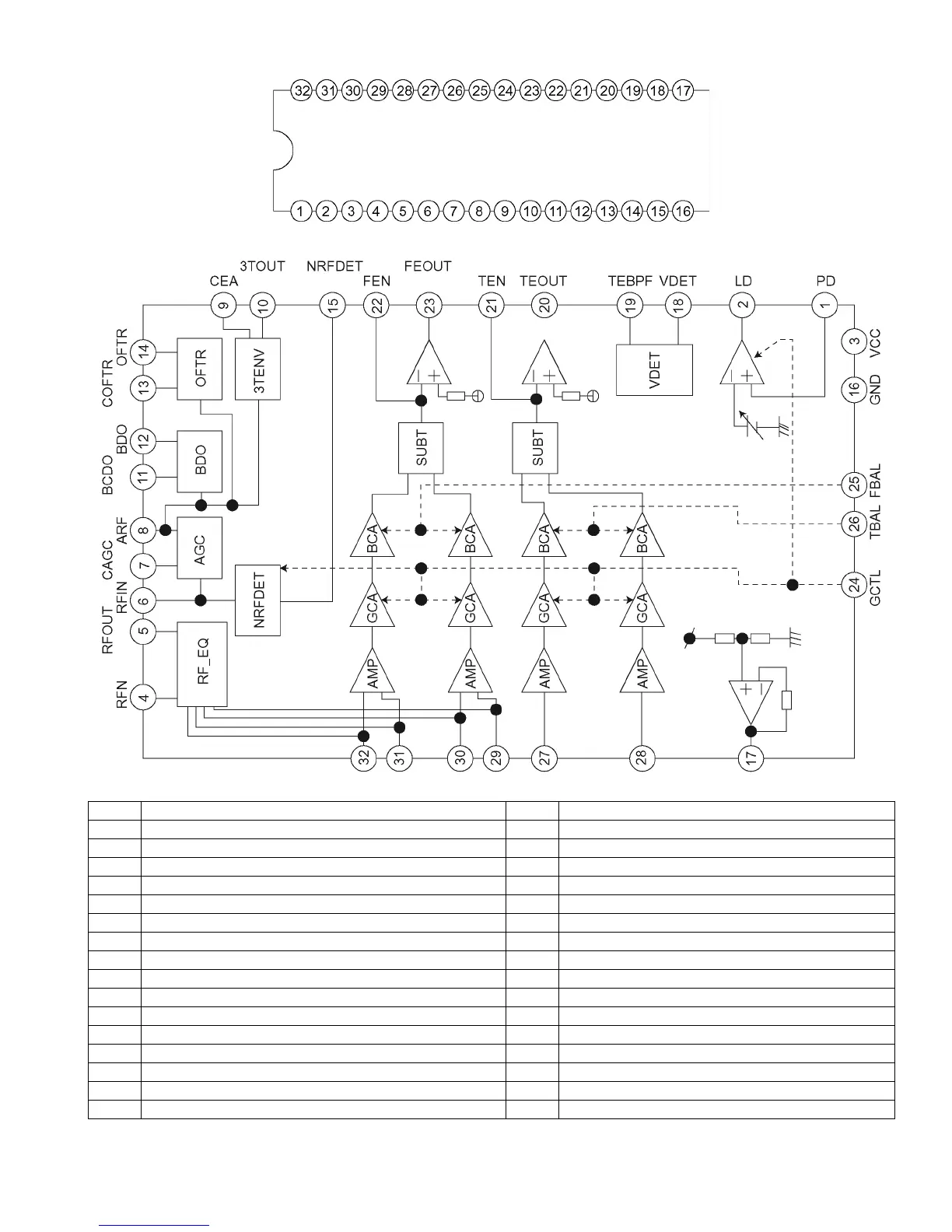
5.12 AN22000A-W (IC601) : RF head amp.
• Pin layout
• Block diagram
• Pin function
Pin No. Function Pin No. Function
1 APC amp input terminal. 17 VREF output terminal.
2 APC amp output terminal. 18 VDET output terminal.
3 Power supply. 19 VDET input terminal.
4 RF amp negative input terminal. 20 TE amp. output terminal.
5 RF amp output terminal. 21 TE amp. negative input terminal.
6 AGC input terminal. 22 FE amp. negative input terminal.
7 AGC loop filter capacitor connection terminal. 23 FE amp. output terminal.
8 AGC output terminal. 24 GCTL & APC terminal.
9 Capacitor connection terminal for HPF-amp. 25 FBAL control terminal.
10 3TENV output terminal. 26 TBAL control terminal.
11 Capacitor connection terminal for RF enberope detection. 27 Tracking signal input terminal 1.
12 BDO output terminal. 28 Tracking signal input terminal 2.
13 Capacitor connection terminal for RF enverope detection. 29 Focus signal input terminal 4.
14 OFTR output terminal. 30 Focus signal input terminal 3.
15 NRDET output terminal. 31 Focus signal input terminal 2.
16 Ground terminal. 32 Focus signal input terminal 1.

 Loading...