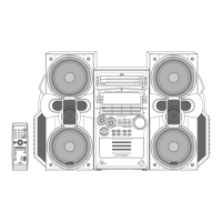
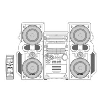
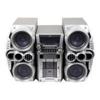
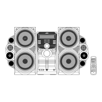
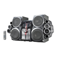
HX-Z1
52
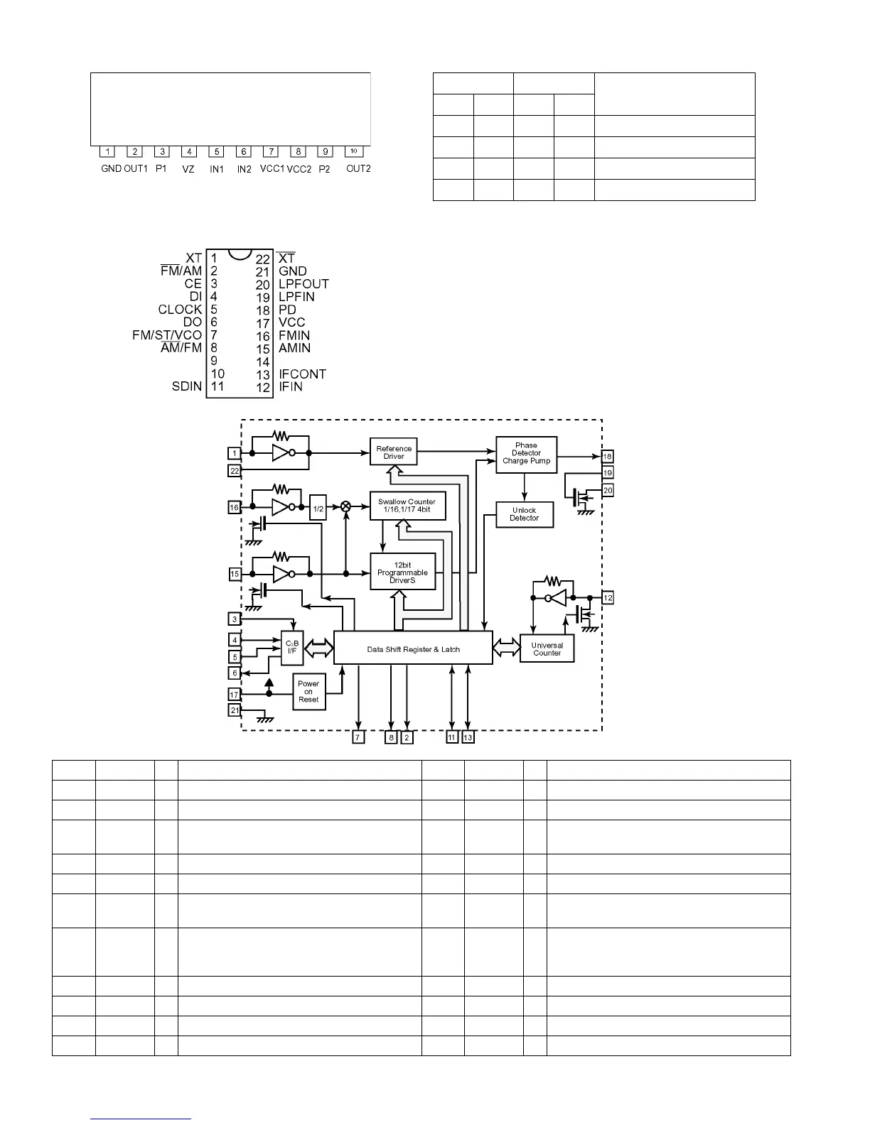
5.20 LB1641 (IC851,IC852) : DC motor driver
• Pin layout • Pin function
5.21 LC72136N (IC2) : PLL frequency synthesizer
• Pin layout
• Block diagram
• Pin function
Input Output Mode
IN1 IN2 OUT1 OUT2
0000Brake
1010CLOCKWISE
0 1 0 1 COUNTER-CLOCKWISE
1100Brake
PinNo. Symbol I/O Function PinNo Symbol I/O Function
1 XT I X'tal oscillator connect (75kHz) 12 IFIN I IF counter signal input
2 FM/AM O LOW:FM mode 13 IFCONT O IF signal output
3 CE I When data output/input for 4pin(input) and
6pin(output): H
14 - Not use
4DII
Input for receive the serial data from controller
15 AMIN I AM Local OSC signal output
5 CLOCK I Sync signal input use 16 FMIN I FM Local OSC signal input
6 DO O Data output for Controller
Output port
17 VCC - Power suplly(VDD=4.5-5.5V)
When power ON:Reset circuit move
7FM/ST/
VCO
O "Low": MW mode 18 PD O PLL charge pump output(H: Local OSC fre-
quency Height than Reference frequency.
L: Low Agreement: Height impedance)
8 AM/FM O Open state after the power on reset 19 LPFIN I Input for active lowpassfilter of PLL
9 LW I/O Input/output port 20 LPFOUT O Output for active lowpassfilter of PLL
10 MW I/O Input/output port 21 GND - Connected to GND
11 SDIN I/O Data input/output 22 XT I X'tal oscillator(75KHz)
 Loading...