(No.YA683<Rev.001>)2-35 2-36(No.YA683<Rev.001>)
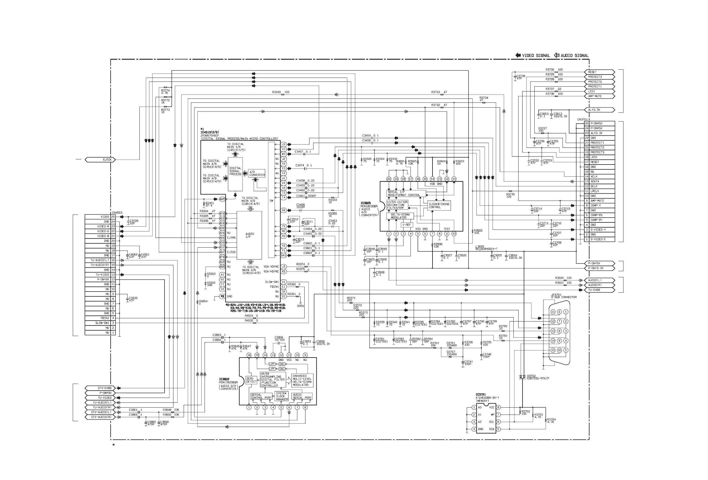
DIGITAL MAIN PWB ASS'Y(2/6)
FU-1ESA19709[LT-19DA1BJ/AK]
FU-1ESA19153[LT-19DA1BU/AK]
A8CN8SCD2_1215_2/6_0.0
The order of pins shown in this diagram is different from that of actual IC4513.
IC4513 is divided into five and shown as IC4513 (1/5) ~ IC4513 (5/5) in this Digital Main Schematic Diagram Section.
1 NOTE:
DIGITAL MAIN PWB CIRCUIT DIAGRAM (2/6)
DIGITAL MAIN PWB(5/6)
DIGITAL MAIN PWB(3/6)
DIGITAL MAIN PWB(6/6)
MAIN PWB(2/3)
CN102A
DIGITAL MAIN PWB(5/6)
DIGITAL MAIN PWB(3/6)
MAIN PWB(1/3)
CN101A
This schematic is only for reference.
Avoid replacing individual parts.
Relpace the entire PWB ASS'Y only.
 Loading...