(No.YA683<Rev.001>)1-9
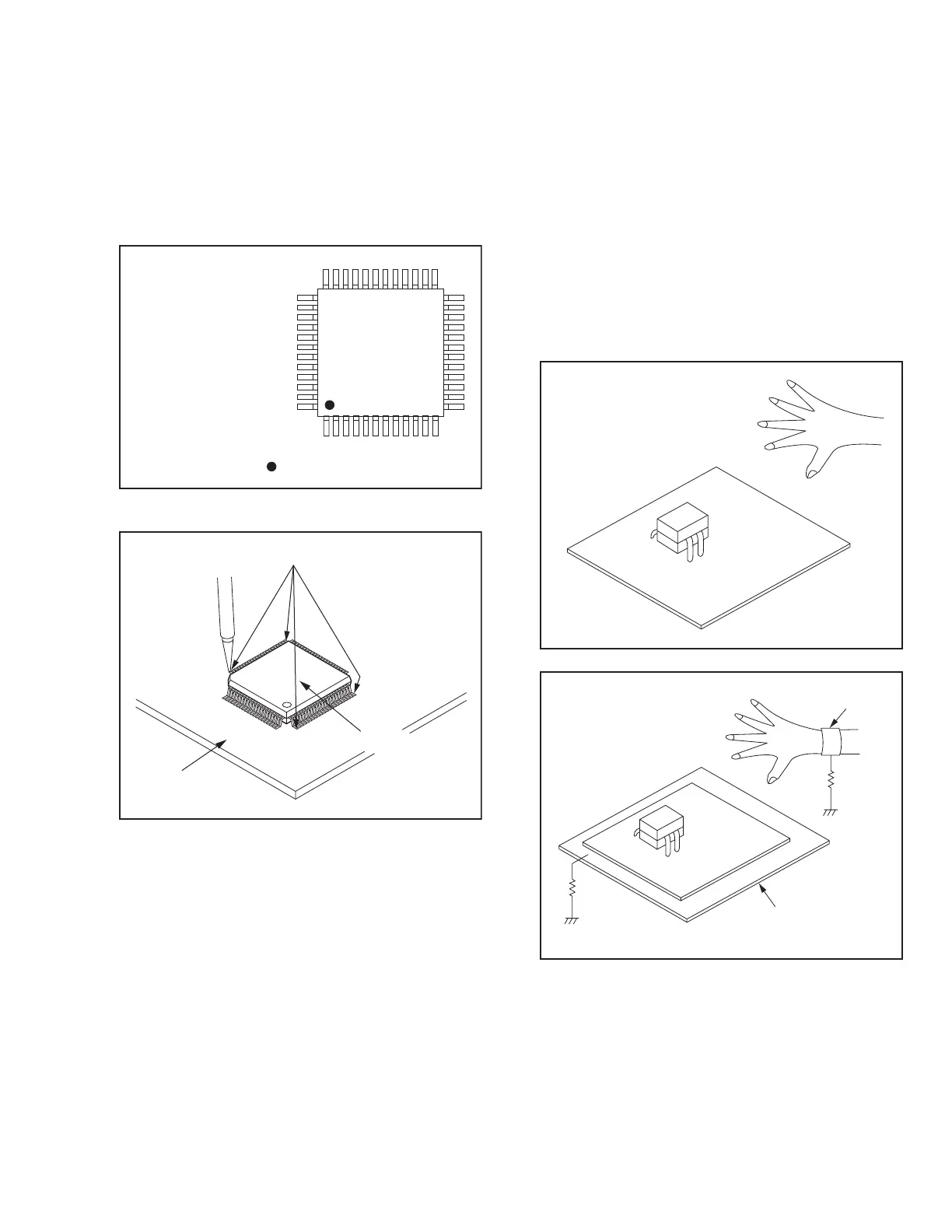
2.3.4.2 INSTALLATION
(1) Using desoldering braid, remove the solder from the foil of
each pin of the flat pack-IC on the PWB so you can install
a replacement flat pack-IC more easily.
(2) The z mark on the flat pack-IC indicates pin 1. (See Fig.2-
7.) Be sure this mark matches the 1 on the PCB when
positioning for installation. Then presolder the four corners
of the flat pack-IC. (See Fig.2-8.)
(3) Solder all pins of the flat pack-IC. Be sure that none of the
pins have solder bridges.
Fig.2-7
Fig.2-8
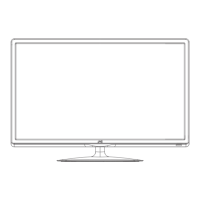
2.3.5 INSTRUCTIONS FOR HANDLING SEMI-
CONDUCTORS
Electrostatic breakdown of the semi-conductors may occur due
to a potential difference caused by electrostatic charge during
unpacking or repair work.
2.3.5.1 GROUND FOR HUMAN BODY
Be sure to wear a grounding band (1MΩ) that is properly
grounded to remove any static electricity that may be charged on
the body.
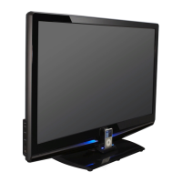
2.3.5.2 GROUND FOR WORKBENCH
Be sure to place a conductive sheet or copper plate with proper
grounding (1MΩ) on the workbench or other surface, where the
semi-conductors are to be placed. Because the static electricity
charge on clothing will not escape through the body grounding
band, be careful to avoid contacting semi-conductors with your
clothing.
Example :
Pin 1 of the Flat Pack-IC
is indicated by a " " mark.
Presolder
CBA
Flat Pack-IC
<I
n
c
o
rr
ec
t
>
CBA
Grounding Band
Conductive Sheet or
Copper Plate
1M
1M
<
C
o
rr
ec
t
>
CBA