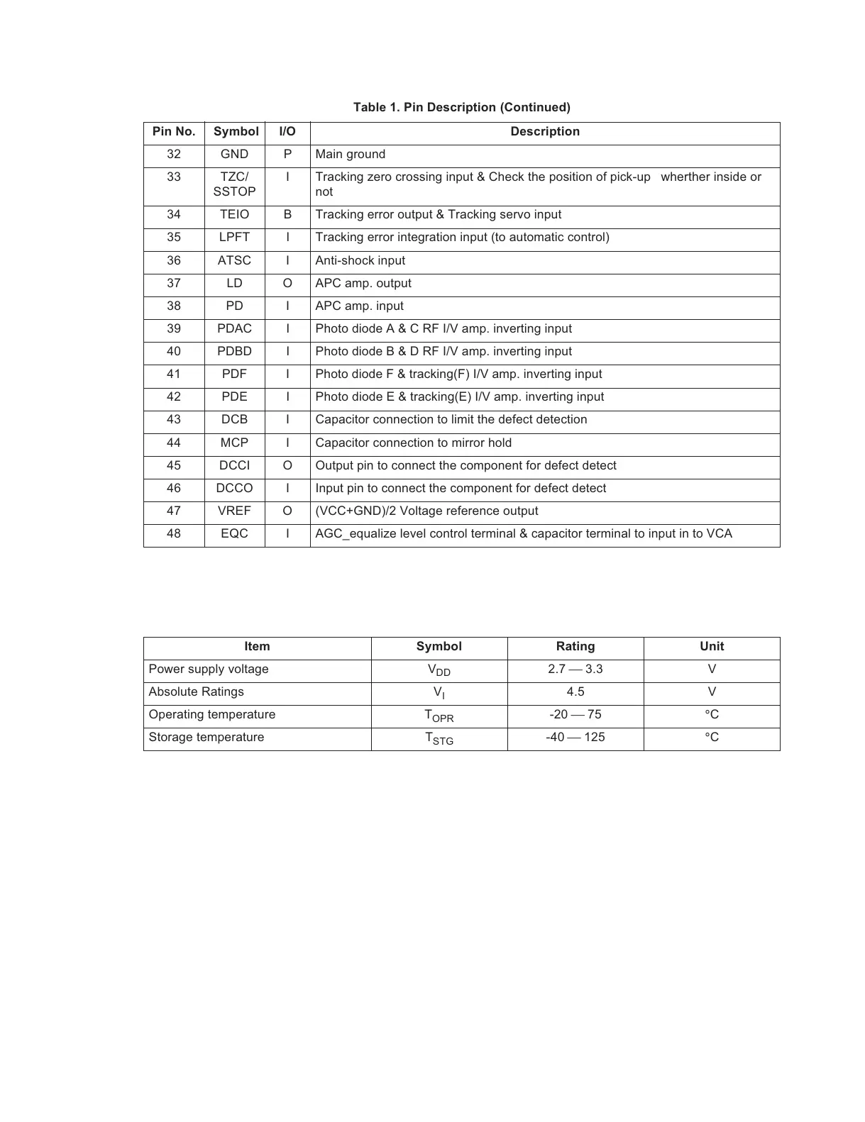
32 GND P Main ground
33 TZC/
SSTOP
I Tracking zero crossing input & Check the position of pick-up
wherther inside or
not
34 TEIO B Tracking error output & Tracking servo input
35 LPFT I Tracking error integration input (to automatic control)
36 ATSC I Anti-shock input
37 LD O APC amp. output
38 PD I APC amp. input
39 PDAC I Photo diode A & C RF I/V amp. inverting input
40 PDBD I Photo diode B & D RF I/V amp. inverting input
41 PDF I Photo diode F & tracking(F) I/V amp. inverting input
42 PDE I Photo diode E & tracking(E) I/V amp. inverting input
43 DCB I Capacitor connection to limit the defect detection
44 MCP I Capacitor connection to mirror hold
45 DCCI O Output pin to connect the component for defect detect
46 DCCO I Input pin to connect the component for defect detect
47 VREF O (VCC+GND)/2 Voltage reference output
48 EQC I AGC_equalize level control terminal & capacitor terminal to input in to VCA
Item Symbol Rating Unit
Power supply voltage V
DD
2.7 3.3 V
Absolute Ratings V
I
4.5 V
Operating temperature T
OPR
-20 75 °C
Storage temperature T
STG
-40 125 °C
Table 1. Pin Description (Continued)
Pin No. Symbol I/O Description
 Loading...