XV-N5SL
28
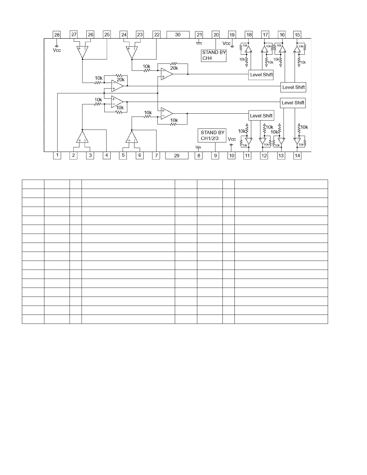
5.2 BA5983FM-X (IC201) : 4CH Driver
5.2.1 Block diagram
5.2.2 Pin function
Pin No. Symbol I/O Description Pin No. Symbol I/O Description
1 BIAS IN I Input for Bias-amplifier 16 VO4(-) O Inverted output of CH4
2 OPIN1(+) I Non inverting input for CH1 OP-AMP 17 VO3(+) O Non inverted output of CH3
3 OPIN1(-) I Inverting input for CH1 OP-AMP 18 VO3(-) O Inverted output of CH3
4 OPOUT1 O Output for CH1 OP-AMP 19 PowVcc2 - Vcc for CH3/4 power block
5 OPIN2(+) I Non inverting input for CH2 OP-AMP 20 STBY2 I Input for Ch4 stand by control
6 OPIN2(-) I Inverting input for CH2 OP-AMP 21 GND - Substrate ground
7 OPOUT2 O Output for CH2 OP-AMP 22 OPOUT3 O Output for CH3 OP-AMP
8 GND - Substrate ground 23 OPIN3(-) I Inverting input for CH3 OP-AMP
9 STBY1 I Input for CH1/2/3 stand by control 24 OPIN3(+) I Non inverting input for CH3 OP-AMP
10 PowVcc1 - Vcc for CH1/2 power block 25 OPOUT4 O Output for CH4 OP-AMP
11 VO2(-) O Inverted output of CH2 26 OPIN4(-) I Inverting input for CH4 OP-AMP
12 VO2(+) O Non inverted output of CH2 27 OPIN4(+) I Non inverting input for CH4 OP-AMP
13 VO1(-) O Inverted output of CH1 28 PreVcc - Vcc for pre block
14 VO1(+) O Non inverted output of CH1 29 - Connect to ground
15 VO4(+) O Non inverted output of CH4 30 - Connect to ground
 Loading...