XV-N5SL
47
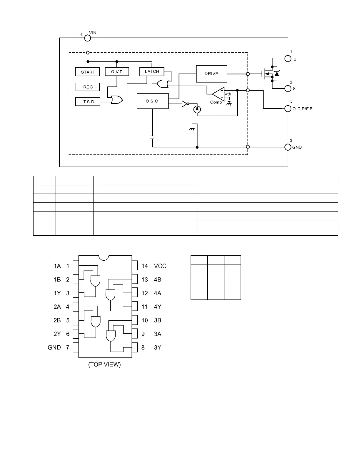
5.14 STR-G6551-F8 (IC901) : Switch regulator
5.14.1 Block diagram
5.14.2 Pin function
5.15 TC74HC08AF-X(IC704) : 2-input and gate
5.15.1 Pin layout 5.15.2 Truth table
Pin No. Symbol Description Function
1 D Drain terminal MOS FET drain
2 S Source terminal MOS FET source
3 GND Ground terminal Ground
4 Vin Power supply terminal Input of power supply for control circuit
5 O.C.P/F.B Over current / Feedback terminal Input of over current detection signal and
constant voltage control signal
ABY
LLL
LHL
HLL
HHH
 Loading...