XV-N5SL
46
5.13 SST39VF160-7CEK (IC509) : 16M EEPROM
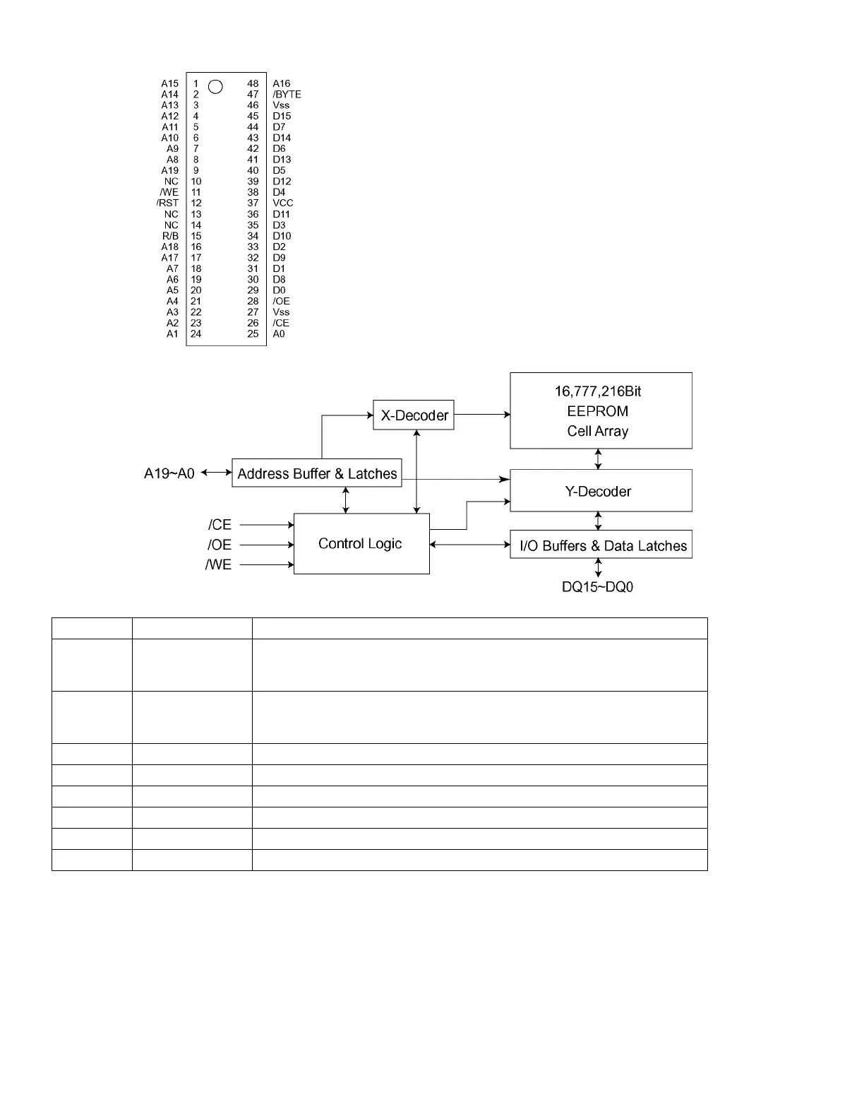
5.13.1 Pin layout
5.13.2 Block diagram
5.13.3 Pin function
Symbol Pin name Function
A19~A0 Address Inputs To provide memory addresses. During sector erase A19~A11 address
lines will select the sector. During block erase A19~A15 address lines
will select the block.
DQ15~DQ0 Data Input/Output To output data during read cycles and receive input data during write
cycles. Data is internally latched during a write cycle. The outputs are
in tri-state when /OE or /CE is high.
/CE Chip Enable To activate the device when /CE is low.
/OE Output Enable To gate the data output buffers.
/WE Write Enable To control the write operations.
VCC Power Supply To provide 3-volt supply ( 2.7V-3.6V ).
Vss Ground
NC No Connection
 Loading...