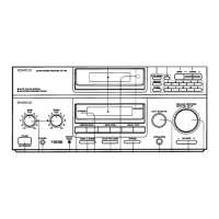
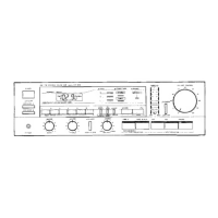
UPD784217GC103(105) (IC1: X14-618X-XX)
System MicroComputer
Pin Pin Name Signal Name I/O Purpose Operation Description
1 P120/RTP0 CHCON O Changer control terminal. ON:Hi, OFF:Lo
2 P121/RTP1 CH_MUTE I Muting input to changer. ON:Hi, OFF:Lo
3 P122/RTP2 REQH O Handshake request to changer.
4 P123/RTP3 DIMMER I Small detection. DIMMER ON:Lo, OFF:Hi
5 P124/RTP4 MOTER O
Cassette mechanism main motor
output.
Active; Hi.
6 P125/RTP5 NC O
7 P126/RTP6 NC O
8 P127/RTP7 NC O
9 Vdd Vdd - Positive power supply.
10 X2 X2 - Main clock connection.
11 X1 X1 - Main clock connection.
12 Vss Vss - GND terminal.
13 XT2 XT2 - Sub-clock connection.
14 XT1 XT1 - Sub-clock connection.
15 RESET RESET I Reset input. Active: Lo.
16 P00/INTP0 CH_RST O Reset output to changer. Active: Hi.
17 P01/INTP1 R_CLK I RDS clock input.
18 P02/INTP2/NMI REQC I Handshake request from changer.
19 P03/INTP3 KEY REQ I
20 P04/INTP4 SUB_MOTOR3 O Sub-motor output. 3
21 P05/INTP5 SUB_MOTOR2 O Sub-motor output. 2
22 P06/INTP6 SUB_MOTOR1 O Sub-motor output. 1
23 AVdd Avdd - A/D analog power supply.
24 AVref0 AVref0 - A/D reference voltage input.
25 P10/ANI0 PHONE I Phone detection.
1 V or less: TEL MUTE
/2.5 V or more: NAVI MUTE.
26 P11/ANI1 SRM_SW1 I SRM position detection. Open: Hi.
27 P12/ANI2 NOISE I FM noise detection.
28 P13/ANI3 SMETER I FM S meter detection.
29 P14/ANI4 F_REEL I
Cassette mechanism reel pulse input
(FWD).
30 P15/ANI5 R_REEL I
Cassette mechanism reel pulse input
(REV).
31 P16/ANI6 N.C. I
32 P17/ANI7 N.C. I
33 AVss AVss - A/D GND terminal.
34 P130/ANO0 EXT_AMP O External amp control.
L 40mS:Bass boost OFF
L 70mS:Bass boost LOW
L 100mS:Bass boost Hi
35 P131/ANO1 IF_MODE I IF status detection for K2I. Hi = WIDE, Lo = NARROW
36 AVref1 AVref1 - D/A reference voltage input.
37 P70/RxD2/SI2 DATAC I Data line from changer.
38 P71/TxD2/SO2 DATAH O Data line to changer.
39 P72/ASCK2/SCK2 CH_CLK I/O Clock line with changer.
40 P20/RxD1/SI1 L_DATAL I Data line from LCD driver.
41 P21/TxD1/SO1 L_DATAS O Data line to LCD driver.
42 P22/ASCK1/SCK1 L_CLK O Clock line to LCD driver.
43 P23/PCL DIMMER O Dimmer control output.
44 P24/BUZ BEEP O Beep output. Active: Hi.
45 P25/SI0 PLL_CE O CE to PLL.
46 P26/SO0 PLL_DATA I/O Data input/output with PLL.
47 P27/SCK0 PLL_CLK O Clock output to PLL.
48 P80/A0 ILL_ON O ILL ON ILL ON : Hi
49 P81/A1 PANEL_5V O
5V power supply control for LCD
driver.
Active: Lo.
50 P82/A2 L_CE O CE terminal to LCD driver
51 P83/A3 LOCK_SW I Panel lock SW detection terminal. Lock SW ON : Lo