2GL/2FV/2FW
2-3-7
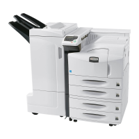
For 16 ppm printer
Figure 2-3-4 Main PWB block diagram (For 16 ppm printer)
The main PWB consists mainly of CPU (U01) and primarily performs the printing data processing and interface controls
with computers. The CPU (U1) outputs the laser light and executes printing following the code ROM (U05) that stores the
control programs being linked with the process and paper feeding/conveying mechanism that the engine/high voltage
PWB controls.
VXIN
CXIN
UXIN
X02
VXOUT
Xtal (video)
37.6687 MHz
X03
YC02
U06
YC03
YC04
YC06
PPDATA8-1
Parallel
I/F
Engine
I/F
APC
I/F
USB
I/F
USBDP
P1284DIR
NSELIN, NSTROBE,
NAUTOFD, NINIT
NACK, PERROR,
SELECT, FAULT, BUSY
USBDN
PDATA7-0
PNSELIN, PNSTROBE,
PNAUTOFD, PNINIT
PNACK, PPERROR,
PSELECT, PFAULT, PBUSY
48.000 MHz
OSC (USB)
(System)
Power source
(+5V SGND)
SCKN, SO, PLGCLK
SBSY, SI, SDIR, EGIRN,
PDMASKN
RESIN
OUTPEN
VDATA
VDFONSPL
PDN
+5V1
SDD31-0
SDRAM d
ata bus
+3.3 V regulator
+3.3V1
U07
SDD31-16
SDCLK
SDRAM
DIMM
slot
SDCLK
IICSCL
SDA12-0
SDA12-0
EBD31-0 EBIU data bus
EBIU address bus
EBA22, EBA10-1
EBD15-1
EBD31-16
EBA21-1
Code
ROM
(Flash
memory)
SDA11-0
SDD31-0 SDD15-0
IICSDA
SDCSN0
SDCSN1-2
U04
SDRAM
U03
SDRAM
YS01
DQMU
SDRAM address bus
DQML
RASN, CASN, WEN, BA1, BA0, SDCLKE
U01
Power PC405
192 MHz
RISC
processor
(Core+ASIC)
YC01
U05
EBA22-1
Memory
card
(optional)
EBCSN2,
EBOEN1, EBWEN1
EBCSN0-1,
EBOEN0, EBWEN0
CDWAITN, CDET
CDRST
IEEE 1284
Transceiver
 Loading...