85
3
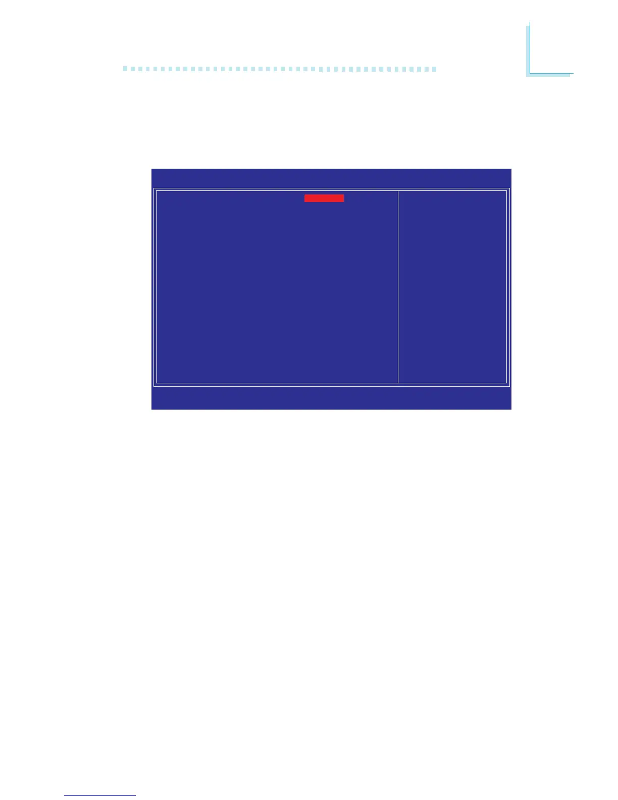
BIOS Setup
DRAM Timing
Move the cursor to this field and press <Enter>. The following
screen will appear.
CAS Latency Time (tCL)
This field is used to select the clock cycle of the CAS latency time.
The option selected specifies the timing delay before SDRAM starts
a read command after receiving it.
Precharge Delay (tRAS)
The options are Auto, and 9 to15.
RAS# Precharge (tRP)
This field is used to select the idle clocks after issuing a precharge
command to the DRAM.
RAS# to CAS# Delay (tRCD)
This field is used to select the RAS# to CAS# delay time when
reading and writing to the same bank.
CAS Latency Time (tCL)
Precharge Delay (tRAS)
RAS# Precharge (tRP)
RAS# to CAS# Delay (tRCD)
Write to PRE Delay (tWR)
REF to ACT Delay (tRFC)
Rank Write to Read (tWTR)
ACT to ACT Delay (tRRD)
Read CAS# Precharge (tRTP)
DIMM 1 CLK Fine Delay
DIMM 2 CLK Fine Delay
DIMM 3 CLK Fine Delay
DIMM 4 CLK Fine Delay
All Precharge to Act
All PRE to Refresh
Phoenix - AwardBIOS CMOS Setup Utility
DRAM Timing
Item Help
Menu Level
XX
↑↓→←: Move Enter: Select F1: General Help+/-/PU/PD: Value F10: Save ESC: Exit
F5: Previous Values F6: Fail-Safe Defaults F7: Optimized Defaults
Auto
Auto
Auto
Auto
Auto
Auto
Auto
Auto
Auto
Current[ 2]
Current[10]
Current[ 0]
Current[14]
Auto
Auto
The settings on the screen are for reference only. Your version may not be
identical to this one.