EasyManuals Logo

Lantronix Qualcomm HDK8450 User Manual

Lantronix Qualcomm HDK8450
42 pages
To Next Page IconTo Next Page
To Previous Page IconTo Previous Page
Page #34 background imageLoading...
Page #34 background image
HDK8450 (SM8450P) Processor User Guide Main board
80-28453-2 Rev. C Confidential Qualcomm Technologies, Inc. and/or its affiliated companies May Contain Trade Secrets 34
MAY CONTAIN U.S. AND INTERNATIONAL EXPORT CONTROLLED INFORMATION
Pin#
Signal
Description
Pin#
Signal
Description
J6201[27]
ALSP_INT_N
GPIO89
J6201[28]
PRESS_INT
GPIO90
J6201[29]
MDP_VSYNC_S
GPIO83
J6201[30]
DISP1_RESET_N
GPIO25
J6201[31]
CAM4_RESET_N
GPIO116
J6201[32]
HALL_INT_N
GPIO80
J6201[33]
CAM5_RESET_N
GPIO115
J6201[34]
SAR_INT_N
GPIO91
J6201[35]
VREG_S10B_1P8
1.8V
J6201[36]
DC_IN
12V
J6201[37]
VREG_5P0
5.0V
J6201[38]
DC_IN
12V
J6201[39]
GND
ground
J6201[40]
GND
ground
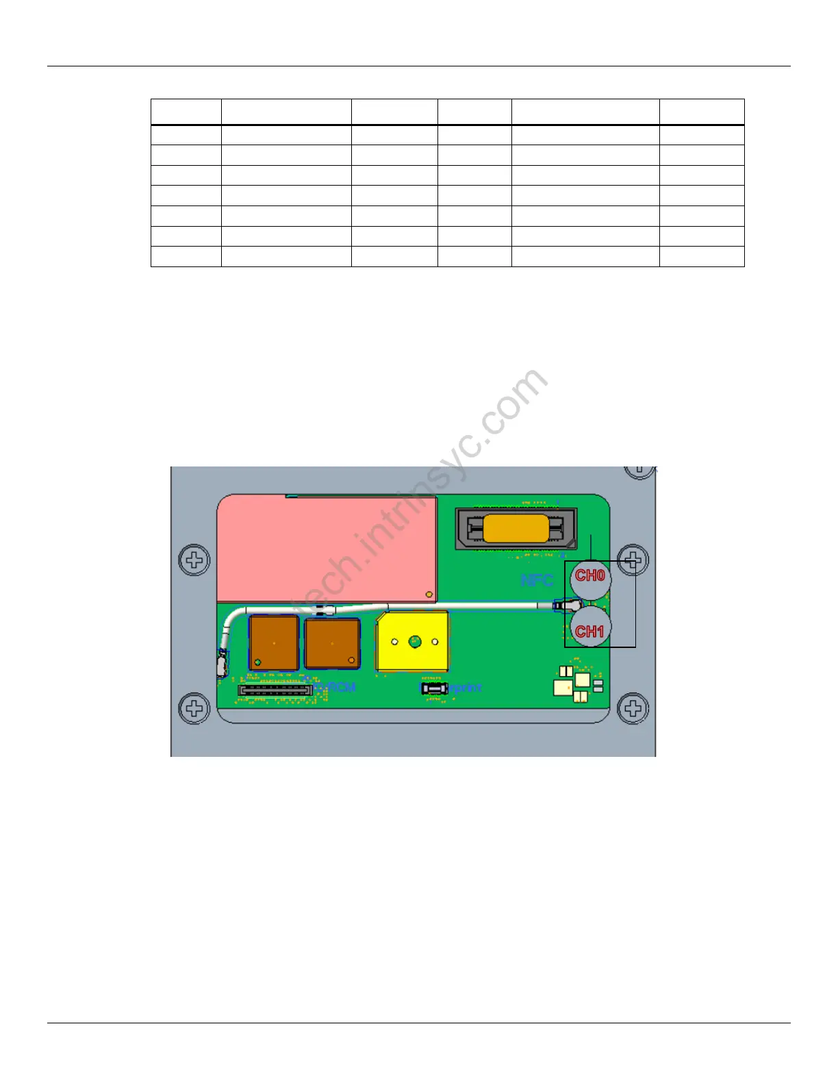
3.4.16 On-board PCB WLAN antenna
The HDK8450 Development Kit has two on-board PCB antennas on the bottom side of the Main
Board.
CH0 is connected to WCN6856 by PCB trace
CH1 is connected to WCN6856 via coaxial cable
CH1 is also connected to GNSS
For better GNSS performance, connect to external antenna via CH1_GNSS test connector
Figure 3-20 On-Board PCB WLAN Antennas
tech.intrinsyc.com
Confidential -- Lantronix, Inc. Lantronix NDA Requir
ed

Table of Contents

Questions and Answers:

Question and Answer IconNeed help?

Do you have a question about the Lantronix Qualcomm HDK8450 and is the answer not in the manual?

Lantronix Qualcomm HDK8450 Specifications

General IconGeneral
BrandLantronix
ModelQualcomm HDK8450
CategoryComputer Hardware
LanguageEnglish