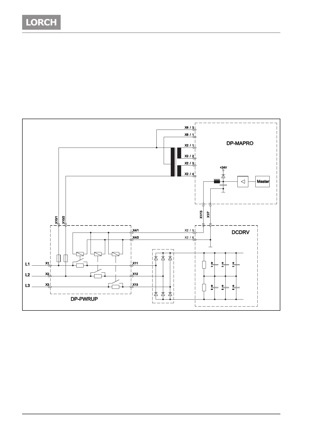
Pc-Boards
- 38 - 02.20909.2710.1-06
Power-up cycle
After switching on the machine with the mains switch, the capacitors on the DCDR pcb are charged up first.
These capacitors are buffering the bus voltage (rectified mains voltage). The input current during charge
up can be very high and must be limited to prevent the mains fuses to break. The current limitation is
made by the PWRUP pcb, where each phase is conducted via resistors to the mains rectifier. After a charge
up time for about two seconds, the resistors on the PWRUP pcb are shorted with the relays, so the the full
mains input is present and the bus voltage is at maximum (560V DC to 580V DC).
The bus voltage is monitored by the DSP (Process) and the relays on the PWRUP board are switched by
the microcontroller (Master).
Schematic
Fig. 26: Power-up circuit