E S I
E S
I
3
Rev. 0A May 25, 2006
ES29LV320E
Excel Semiconductor inc.
PRODUCT SELECTOR GUIDE
Family Part Number ES29LV320E
Voltage Range 2.7V ~ 3.6 V
Speed Option 70 90
Max Access Time (ns) 70 90
CE# Access (ns) 70 90
OE# Access (ns) 30 40
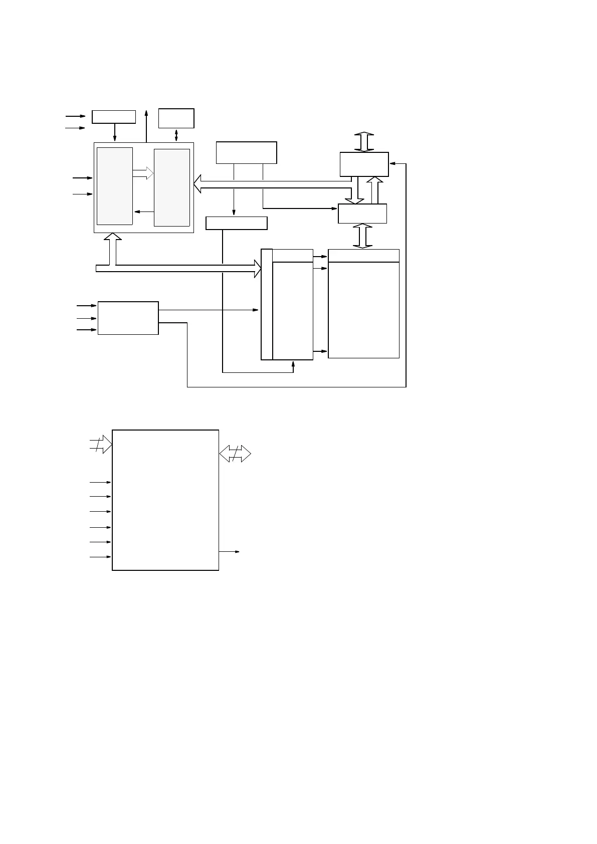
Command
Register
Analog Bias
Generator
Address Latch
BYTE#
CE#
OE#
A<0:20
>
RESET#
Vcc
Vss
Chip Enable
Output Enable
Logic
Vcc Detector
Timer/
Counter
Y-Decoder
X-Decoder
Y-Decoder
Cell Array
Data Latch/
Sense Amps
Input/Output
Buffers
Sector Switches
DQ0-DQ15(A-1)
RY/BY#
Write
State
Machine
WE
#
FUNCTION BLOCK DIAGRAM
E S I
E S
I
4
Rev. 0A May 25, 2006
ES29LV320E
Excel Semiconductor inc.
PIN DESCRIPTION
Pin Description
A0-A20 21 Addresses
DQ0-DQ14 15 Data Inputs/Outputs
DQ15/A-1
DQ15 (Data Input/Output, Word Mode)
A-1 (LSB Address Input, Byte Mode)
CE# Chip Enable
OE# Output Enable
WE# Write Enable
WP#/ACC Hardware Write Protect/Acceleration Pin
RESET# Hardware Reset Pin, Active Low
BYTE# Selects 8-bit or 16-bit mode
RY/BY# Ready/Busy Output
Vcc
3.0 volt-only single power supply
(see Product Selector Guide for speed options and voltage supply tolerances)
Vss Device Ground
NC Pin Not Connected Internally
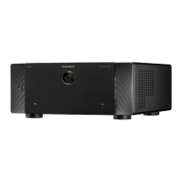
LOGIC SYMBOL
DQ0 ~ DQ15
(A-1)
RY/BY#
BYTE#
RESET#
OE#
CE#
A0 ~ A20
WP#/ACC
WE#
21
16 or 8