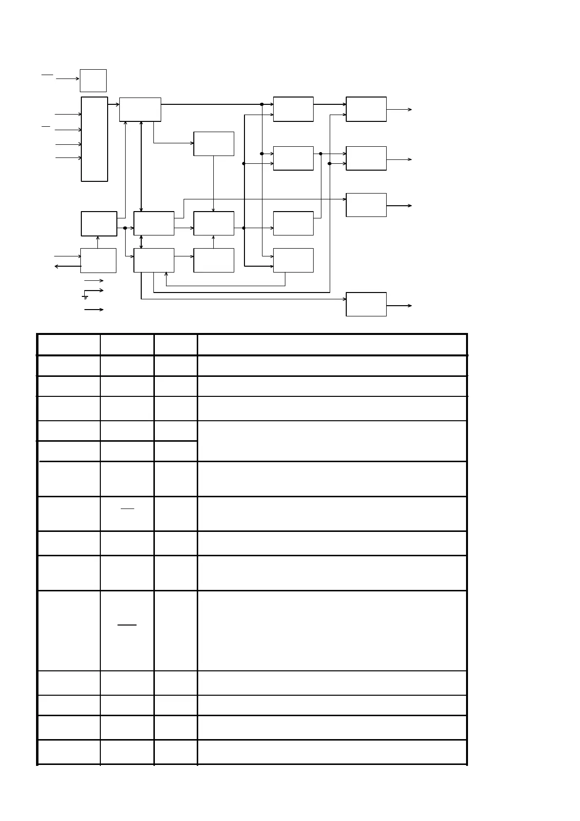
N o . S Y M B O L I/O F U N C T I O N
5 7 V D D - P o w er S o u r ce : V D D = +3 .0 to 5 . 5 V
4 9 V S S - G N D : V S S =0 V
4 8 V F D P -
V F D D r i v i n g P o w e r S o u r s e
V
D D -2 0 V t o V D D - 4 5V
5 0 O S C 1 I
CR O s cil l a tio n Ter m ina l
Ext e r n a l R and C connect to these t e r minals.
(Target f
O S C = 3 6 0k Hz )
5 1 O S C 2 O
5 4 C L K I
Serial Clock I n p u t Terminal
Th e serial dat a input sync h ronizing t h e rise edge o f this
terminal.
5 3 C S I
Chip Sel e c t T e rmin a l
When th e C S t ermi n a l is "H" t h e s eri
al data i n put is no t
available.
5 5 S I I
Serial Data Inpu t Term i n al
The d a t a i n p u t i s MSB first.
5 6 R S I
Register Selection Signal I n p u t Terminal
RS="0 " : Instruction Reg ister
R S =" 1 " : D a t a R e gi s t e r
5 2 R S T I
Re s e t T e r m in al R S T = "L " : R e se t
- E a c h A d d r e s s
- Ea c h R A M D at a
- Dis p la y Di g its
- Contr a st C o ntrol
-All Display Off
-All Outputs are "L"
: (00)
H
: Unfixed
: 1 6 - d i g i t
: 8/16 Dury
61 t o 6 4 ,
1 t o 3 1
S
1 to S 3 5 O
Segment Output Terminals (Internal Pull-down
Re si st an ce )
32 t o 4 7 T1 to T1 6 O Timing Output Terminals (Internal Pull-down Resista nce)
6 0
5 9
M K 1
M K 2
O Icon Output Terminals (Internal Pull-down Resistance)
5 8 P 1 O
Ou tput Port T e rminal
This t e rmina l is s u i table for L E D .