2018 Microchip Technology Inc. DS70005340A-page 15
CAN FD Protocol Module
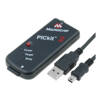
Register 3-7: C1TDCH: CAN Transmitter Delay Compensation Register High
(1)
U-0 U-0 U-0 U-0 U-0 U-0 R/W-0 R/W-0
— — — — — — EDGFLTEN SID11EN
bit 15 bit 8
U-0 U-0 U-0 U-0 U-0 U-0 R/W-1 R/W-0
— — — — — — TDCMOD1 TDCMOD0
bit 7 bit 0
Legend:
R = Readable bit W = Writable bit U = Unimplemented bit, read as ‘0’
-n = Value at POR ‘1’ = Bit is set ‘0’ = Bit is cleared x = Bit is unknown
bit 15-10 Unimplemented: Read as ‘0’
bit 9 EDGFLTEN: Enable Edge Filtering During Bus Integration State bit
1 = Edge filtering is enabled according to ISO11898-1:2015
0 = Edge filtering is disabled
bit 8 SID11EN: Enable 12-Bit SID in CAN FD Base Format Messages bit
1 = RRS is used as SID11 in CAN FD base format messages: SID<11:0> = {SID<10:0>, SID11}
0 = Does not use RRS; SID<10:0>
bit 7-2 Unimplemented: Read as ‘0’
bit 1-0 TDCMOD<1:0>: Transmitter Delay Compensation mode bits (Secondary Sample Point (SSP))
10-11 = Auto: Measures delay and adds TSEG1<4:0> (C1DBTCFGH<4:0>); add TDCO<6:0>
01 = Manual: Does not measure, uses TDCV<5:0> + TDCO<6:0> from register
00 = Disables
Note 1: This register can only be modified in Configuration mode (OPMOD<2:0> = 100).