© 2009 MIMAKI ENGINEERING CO.,LTD.
2.3.2 P.2
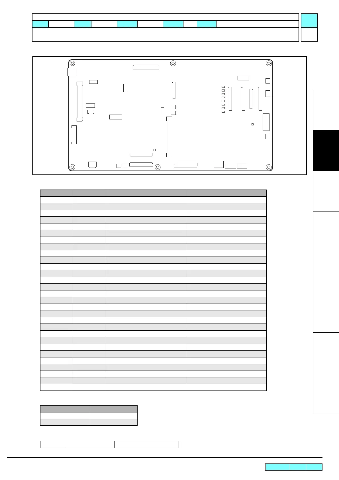
2.3.2 Main PCB Assy
1
2
3
4
5
6
7
8
List of connectors
Test poi nt
Fuse rating
CN No Pin Connected to: Remarks
CN1 30 Ink Slider PCB Assy Head, IO signal
CN2 50 Ink Slider PCB Assy Head signal
CN3 30 Ink Slider PCB Assy Power source
CN4 30 Ink Slider PCB Assy COM drive
CN5 6 Power Supply PCB Assy Heater control
CN6 6 Debug Monitor FPGA/CPLD writing
CN7 80 PRAM PCB Assy
CN8 50 Cutter Driver PCB Assy Control signal
CN9 6 Debug Monitor FPGA
CN10 8 Cutter Driver PCB Assy Power source
CN11 4 USB I/F USB2.0
CN12 80 AUX. Extension IF PCB Assy
CN13 5 AUX. Extension IF PCB Assy
CN14 40 Station PCB Assy
CN15 30 X-axis Motor Relay PCB Assy
CN16 28 X-axis Motor Relay PCB Assy
CN17 10 Regenerative Resistivity PCB Assy
CN18 2 HDC Fan
CN19 2 AUX. AUX.
CN20 3 AUX.
CN21 7 Thermistor Media heater temperature detection
CN22 4 Serial Debug Monitor AUX.
CN23 100 Debug Board FW program writing
CN24 18 Power Supply PCB Assy
CN25 5 Y-axis Motor Encoder
CN26 8 G/A Debug Monitor AUX.
CN27 3 Y-axis Motor
CN28 4 Not used
CN29 2 X-axis Motor
Terminal name Application
GND2, 6 GND
TP1-8 COM voltage (1-8)
F13 0.375A/ 125V 42 V power supply for heads
CN11
CN6
CN23
CN25
CN28
CN26
CN17
CN27
CN7
CN9
CN8
CN1
CN20
F13
CN24
CN19
CN2
CN3
CN5CN21
CN18
GND2
GND6
CN10
CN14
CN15
CN29
CN16
TP8
TP7
TP6
TP5
TP4
TP3
TP2
TP1
CN4
CN12
CN13
CN22
R.1.1
Maintenance Manual > Electrical Parts > Circuit Board Specifications > Main PCB Assy
Model CJV30/TPC Issued 2008.08.04 Revised 2008.09.17 F/W ver. 1.20 Remark
1.1
 Loading...