© 2009 MIMAKI ENGINEERING CO.,LTD.
2.3.2 P.1
1
2
3
4
5
6
7
8
R.1.0
Maintenance Manual > Electrical Parts > Circuit Board Specifications > Main PCB Assy
Model CJV30/TPC Issued 2008.08.04 Revised F/W ver. 1.00 Remark
1.0
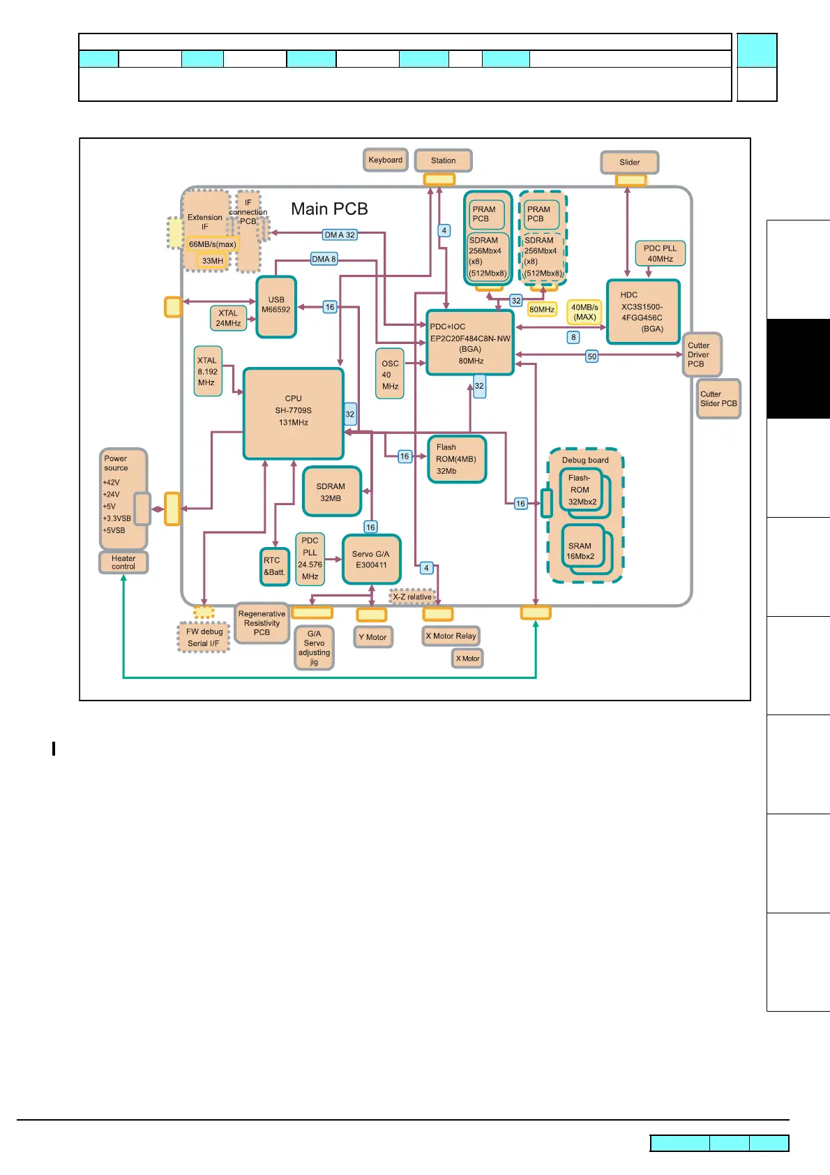
2.3.2 Main PCB Assy
Outline
Board name: Main PCB Assy
The CPU used is SH-3 (RISC, 133MHz) made by Hitachi.
A program for the CPU is written in flash memory. Version up of this program is easily executed on site through I/F.
The version up is carried out by downloading the program to PRAM through CPU and then by writing it in the flash
memory.
When received data is read from I/F, the CPU writes the data in PRAM through PDC. Then the data, after being
subjected to required processes by PDC-CTR, is transmitted to the HDC.
Receiving the data, the HDC creates head driving COM signals and nozzle data, and then transmits each data to the
ink slider PCB assy via HDC FFC cable.
In case of printing by the use of pens and cutters, when the main PCB assy receives a command from I/F to
implement printing, it buffers the command to a memory for exclusive use (32MB SDRAM) and starts printing by
analyzing the command.
The main PCB assy also has X, Y-axis motor driving circuit and other I/O control circuits.
 Loading...