Theory of Operation
2-31
2.9.4 Synthesizer Operation
The complete synthesizer subsystem comprises mainly of a low voltage FRAC-N (LVFRACN)
IC
,
Reference Oscillator (crystal oscillator with temperature compensation), charge pump circuits, loop
filter circuits, and de supply. The output signal
(PRESC_OUT) of the VCOBIC (U3301, pin12)
is
fed
to
of
U3201, pin 32 (PRE IN) via a low pass filter (L3205 and C3246) which attenuates harmonics
and provides correct level
to
close the synthesizer loop.
The
pre-scaler in the synthesizer (U3201) is basically a dual modulus pre-scaler with selectable
divider ratios. The divider ratio
of
the pre-scaler
is
controlled by the loop divider, which in turn
receives its inputs via the SRL. The output
of
the pre-scaler
is
applied to the loop divider. The output
of
the loop divider
is
connected to the phase detector, which compares the loop divider's output
signal with the reference signal. The reference signal
is
generated by dividing down the signal of the
reference
oscillator (Y3201).
The output signal
of
the phase detector is a pulsed
de
signal which
is
routed
to
the charge pump.
The charge pump outputs a current at pin 43
of
U3201 (lOUT). The loop filter (which consists
of
R3214-15, R3218, C3235-7, C3245 and L3204) transforms this current into a voltage that is applied
to the varactor diodes
CR3303 for transmit, CR3301-2 for receive and alters the output frequency
of
the VCO.The current can be set to a value fixed
in
the LVFRAC-N
IC
or
to a value determined by the
currents flowing into
BIAS 1 (U3201-40) or BIAS 2 (U3201-39). The currents are set
by
the value
of
R3211 or R3213 respectively. The selection
of
the three different bias sources is done by software
programming.
LOCK (U3201-4) signal
is
routed to one
of
the
J,JP's
ADCs input U101-56. From the voltage the
J,JP
determines whether LOCK is active.
In order to modulate the PLL the two spot modulation method
is
utilized Via pin 10 (MODIN) on
U3201. The audio signal is applied to both the
AID converter (low frequency path) as well as the
balanced attenuator (high frequency path). The
AID converter converts the low frequency analog
modulating signal into a digital code which is applied to the loop divider, thereby causing the carrier
to
deviate. The balance attenuator is used
to
adjust the VCO's deviation sensitivity to high frequency
modulating signals. The output of the balance attenuator
is
present at the MODOUT port (U3201-
41) and connected to the steering line via R3219-20 and C3241.
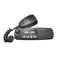
2.10 Control Head (CDM1550•LS+)
The control head contains the internal speaker, the on/off/volume knob, the microphone connector,
several buttons to operate the radio, several indicator light emitting diodes (LEOs) to inform the user
about the radio status, and a 14 character liquid crystal display (LCD) for alpha - numerical
information, e.g. channel number or
call address name.
To
control the LED's and the LCD, and to
communicate with the host radio the control head uses the Motorola 68HC11 E9
J,JP.
2.10.1 Power Supplies
The power supply to the control head is taken from the host radio's
FLT
A+ voltage via connector
J0801 pin 3 and the regulated +5V via connector J0801 pin
7.
The voltage FLT A+
is
at battery level
and is used for the LED's, the back light and
to
power up the radio via on I off I volume knob. The
stabilized +5 volt
is
used for the
J.JP,
display, display driver, and keypad buttons. The voltage USW 5V
derived from the
FLT
A+ voltage and stabilized by the series combination
of
R0822, VR0822 is used
to
buffer the internal RAM
of
the
J,JP
(U0831
).
C0822 allows the battery voltage to be disconnected
for a couple
of
seconds without losing RAM parameters. Dual diode
00822
prevents radio circuits
from discharging this capacitor. When the supply voltage
is
applied to the radio, C0822
is
charged
via
R0822 and 00822.
To
avoid that the
J.JP
enters the wrong mode when the radio
is
switched on
while the voltage across
C0822
is
still
too
low, the regulated 5V charge C0822 via diode
00822
.

 Loading...