iii
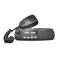
2.10 Control Head (COM 1550•LS+) ..........................................................................
2-31
2.1
0.1
Power Supplies .....................................................................
..
.....
........
2-31
2.10.2 Power
On
I Off ............... ............................................................... .
...
.
..
2-32
2.1
0.3 Microprocessor Circuit .................................
..
..................
..
.................. 2-32
2.10.4 SBEP Seriallnterface ...................................................
....
......
...
.......... 2-32
2.1
0.5 Keypad Keys ..........................................
...
...........................
..
.
...
.. ..
...... 2-33
2.10.6
Status LED
and
Back Light Circuit.. ..............
..
......................
..
..
...
........ 2-33
2.1
0.
7 Liquid Crystal Display (LCD) ................................................................ 2-33
2.1
0.8 Microphone Connector Signals ........................................................
..
..
2-34
2.1
0.9 Speaker ................................................................................
..
..
............ 2-35
2.1
0.1
0 Electrostatic Transient Protection
..
.......
..
....................
.....
............
.. ..
..
..
2-35
2.11
PassPort Trunking Controller Board (PTCB)
.. ..
.
..
.... ....
....................................
..
2-35
Chapter 3 Maintenance
3.1
Introduction ......................................................................
..
..................................
3-1
3.2 Preventive Maintenance
..
...
....
........................
..
.............
...
..
...
...
...........................
3-1
3.2.1
Inspection ................................
...
............................
..
.
..
...........................
3-1
3.2.2 Cleaning ...........
..
....... .........
...
...........
..
...
..
.......
..
.........
..
.........................
..
3-1
3.3 Safe Handling of CMOS and LDMOS ................................
..
....
.
..
..
.............
..
.....
..
. 3-2
3.4 General Repair Procedures
and
Techniques ........................
....
.....
....
..
..
....
.
....
..
..
3-2
3.5 Recommended Test
Tools .......
..
.
...
.......................................... ................
...
..
.. ..
...
3-5
3.6 Receiver
Troubleshooting Chart (200 MHz) ..............................................
..
....
.. ..
3-6
3.7 Receiver Troubleshooting Chart (700 MHz) ............
..
..........
....
........
..
.....
..
..
.. ..
..... 3-8
3.8 Transmitter
Troubleshooting Chart (200 MHz) ............................
..
..................
..
3-10
3.9 Transmitter Troubleshooting Chart (700 MHz) ..................................................
3-11
3.10 Synthesizer Troubleshooting Chart (200 MHz) ............
..
...
..
............................... 3-12
3.11
Synthesizer Troubleshooting Chart (700 MHz) .............
.. ..
..............
...
.......
..
..
...
..
3-13
3.12
VCO Troubleshooting Chart (200 MHz) ............................................................. 3-15
3.13 VCO Troubleshooting Chart (700 MHz) ......................................
....
.....
..
............ 3-16
Chapter 4
Schematic Diagrams, Overlays,
and
Parts Lists
4.1
Introduction .......................................
..
...............................................................
..
4-1
4.1.1 Notes For All Schematics
and
Circuit Boards ........................................
4-1
Figure 4-1. CDM1550•LS+ Control Head Top Overlay .....................................
..
...
4-3
Figure 4-2. CDM1550•LS+ Control Head Bottom Overlay ........... ......................
..
..
4-4
Figure 4-3.
CDM1550•LS+ Control Head Schematic Diagram .......
..
...............
..
..... 4-5
Figure 4-4.
CDM1550•LS+ Control Head Keypad Schematic ................................ 4-6
Figure 4-5. CDM1550•LS+ Control Head Backlight Schematic
...
..
...............
..
........ 4-7
Figure 4-6.
CDM1550•LS+ Control Head Display Schematic .....
..
......................... 4-8
CDM1550•LS+ Control Head Parts List.. ..................................................................... 4-9
Figure 4-7. 200 MHz Main Board Top Side PCB ........................ .......
...
..
..
........... .4-11
Figure 4-8.
200
MHz Main Board Bottom Side PCB ...................................
.. ..
..
..
.4-12
Figure 4-9.
200 MHz Receiver Front
End
Schematic Diagram ..............
..
..
..
........ 4-13

 Loading...