Appendix B Timing Diagrams
© National Instruments Corporation B-19 M Series User Manual
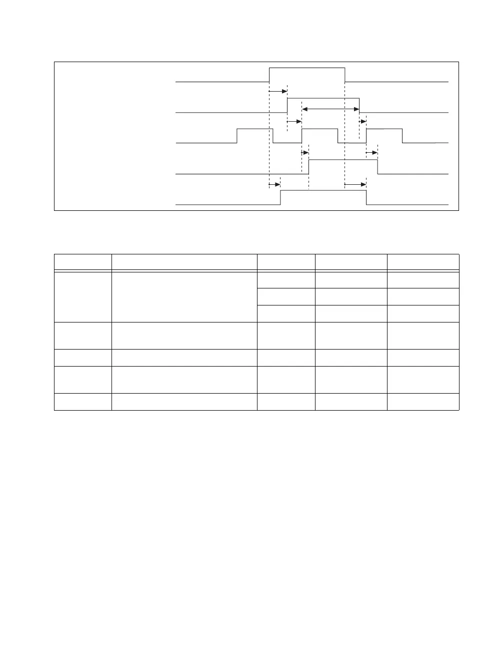
Figure B-19. Pause Trigger Timing Diagram
Output Timing
Output timing refers to the delays involved in exporting internal signals to
external terminals, so they can be used to trigger or time external devices.
These timing parameters include the selection multiplexer in each terminal
plus the delay of the output driver. Figures B-20 and B-21 and Table B-11
describe output timing.
The delays presented in this section assume a 200 pF load on PFI lines and
a 50 pF load on RTSI lines. Actual delays will vary with the actual load.
Table B-10. Pause Trigger Timing
Time Description Line Min (ns) Max (ns)
t
34
_i to Selected Gate PFI 3.2 7.8
RTSI 3.0 7.5
STAR 2.5 4.9
t
35
Selected Pause Trigger Setup Time
(to Sync Convert Clock Timebase)
— 1.5 —
t
36
Hold (Sync Convert Clock Timebase) — 0 —
t
37
Sync Convert Clock Timebase
to Pause Trigger
— 0.6 2.6
t
38
Pause Trigger Source in _i to POUT RTSI 1.1 3.1
_i
POUT
Selected Pause Trigger
Sync Convert Clock Timebase
Pause Trigger
t
34
t
36
t
37
t
37
t
37
t
35
t
35
t
38
 Loading...