Appendix B Timing Diagrams
© National Instruments Corporation B-33 M Series User Manual
Digital Waveform Generation Timing
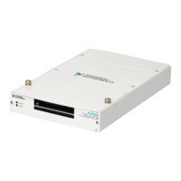
To describe digital waveform generation timing delays and requirements,
we model the circuitry as shown in Figure B-39. In the figure, P0, PFI,
RTSI, and PXI_STAR represent signals at connector pins of the M Series
device. The other named signals represent internal signals.
Figure B-39. Digital Waveform Generation Timing Circuitry
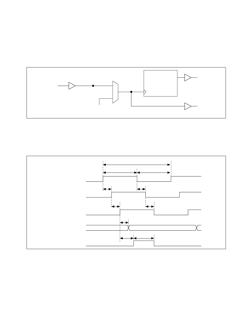
Figure B-40 and Tables B-24 and B-25 describe the digital waveform
generation timing delays and requirements. Your inputs must meet the
requirements to ensure proper behavior.
Figure B-40. Digital Waveform Acquisition Timing Delays
DO Waveform
Generation FIFO
PFI (Output)
P0
DO Sample
Clock
Other Internal
Signals
PFI_i, RTSI_i,
or PXI_STAR_i
PFI, RTSI,
or PXI_STAR
PFI, RTSI,
or PXI_STAR
PFI_i, RTSI_i,
or PXI_STAR_i
DO Sample Clock
P0
PFI (Output)
t
10
t
11
t
12
t
12
t
11
t
13
t
13
t
15
t
16
t
14
 Loading...