Peak 650 User's Guide Rev. A October 2000
BIOS Setup
4-35
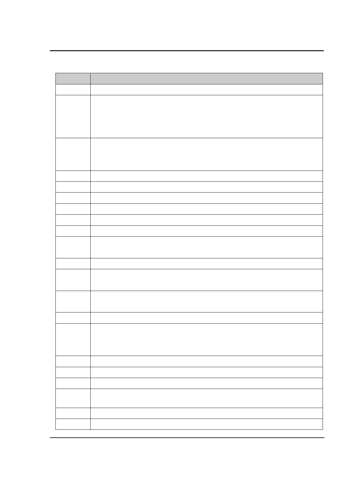
4-3 BIOS Reference - POST Codes
POST (hex) Description
CFh Test CMOS R/W functionality.
C0h Early chipset initialization:
-Disable shadow RAM
-Disable L2 cache (socket 7 or below).
-Program basic chipset registers.
C1h Detect memory
-Auto-detection of DRAM size, type and ECC.
-Auto-detection of L2 cache (socket 7 or below).
C3h Expand compressed BIOS code to DRAM.
C5h Call chipset hook to copy BIOS back to E000h & F000h shadow RAM..
01h Expand the Xgroup codes locating in physical address 1000h:0.
02h Reserved.
03h Initial Superio_Early_Init switch.
04h Reserved.
05h 1. Blank out screen.
2. Clear CMOS error flag.
06h Reserved.
07h 1. Clear 8042 interface.
2. Initialize 8042 self-test.
08h 1. Test special keyboard controller for Winbond 977 series Super I/O chips.
2. Enable keyboard interface.
09h Reserved.
0Ah 1. Disable PS/2 mouse interface (optional).
2. Auto detect ports for keyboard & mouse followed by a port & interface swap (optional).
3. Reset keyboard for Winbond 977 series Super I/O chips.
0Bh Reserved
0Ch Reserved
0Dh Reserved
0Eh Test F000h segment shadow to see whether it is R/W-able or not. If test fails, keep beeping
the speaker.
0Fh Reserved
10h Auto detect flash type to load appropriate flash R/W codes into the run time area in F000