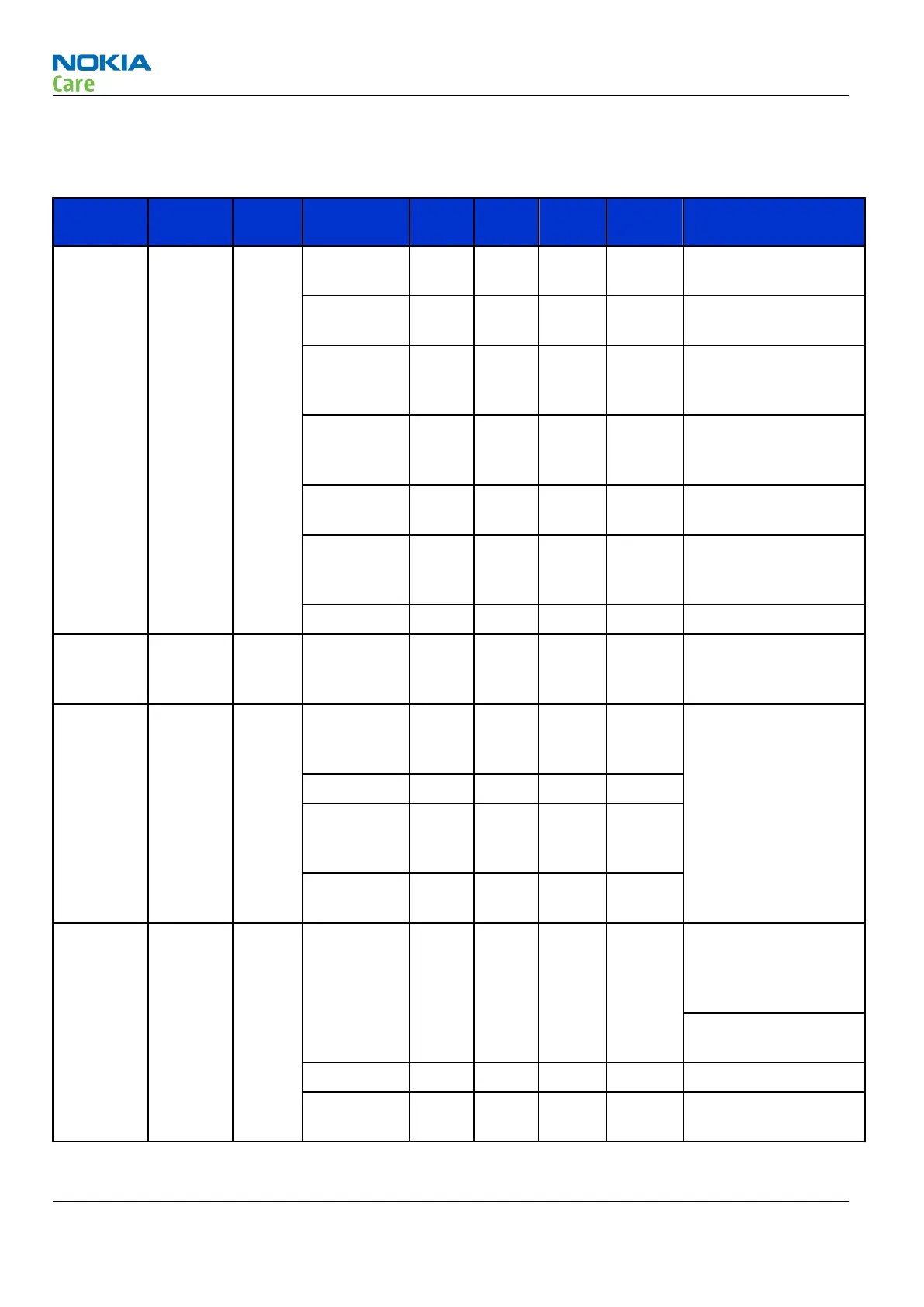
Analogue Signals
Table 9 AC and DC Characteristics of RF-Base band Analogue Signals
Signal
name
From To Parameter Min Typ Max Unit Function
RFCLK VCTCXO UPP Frequency 13/26 MHz System Clk from RF to
BB,
Signal
amplitude
0.2 0.8 1.32 Vpp 13/26 MHz Depending
on RF chipset
Input
Impedance
10 kW UPP minimum
recommended
amplitude is 0.3Vpp.
Input
Capacitanc
e
10 pF
Harmonic
Content
-8 dBc
Clear signal
window
(no glitch)
200 mVpp
Duty Cycle 40 60 %
RFCLKGnd VCTCXO UPP DC Level 0 V System Clock slicer Ref
GND, not separated
from pwb GND layer
RXIP,
RXIN,
RXQP,
RXQN
RF-IC UEMCL
ite
Voltage
swing
(static)
1.4 1.45 Vpp Differential positive /
negative in-phase
and quadrature Rx
Signals.
DC level 1.3 1.35 1.4 V
I/Q
amplitude
mismatch
0.2 dB
I/Q phase
mismatch
-0.5 0.5 deg
TXIP,
TXIN,
TXQP,
TXQN
UEMCLit
e
RF-IC Differential
voltage
swing
(static)
2.25 2.45 Vpp Differential positive /
negative in-phase
and quadrature Tx
Signals
In High-Z when RX is
receiving.
DC level 1.17 1.20 1.23 V
Source
Impedance
200 W
RM-340; RM-341
System Module
Page 6 –14 COMPANY CONFIDENTIAL Issue 1
Copyright © 2007 Nokia. All rights reserved.