PCIe Compliance Testing Reference
PRELIMINARY INFORMATION
Jetson AGX Orin Series Tuning and Compliance Guide DA-11040-001_v0.7 | 14
Figure 2. Use of CBB as a Mode Pulse Generator
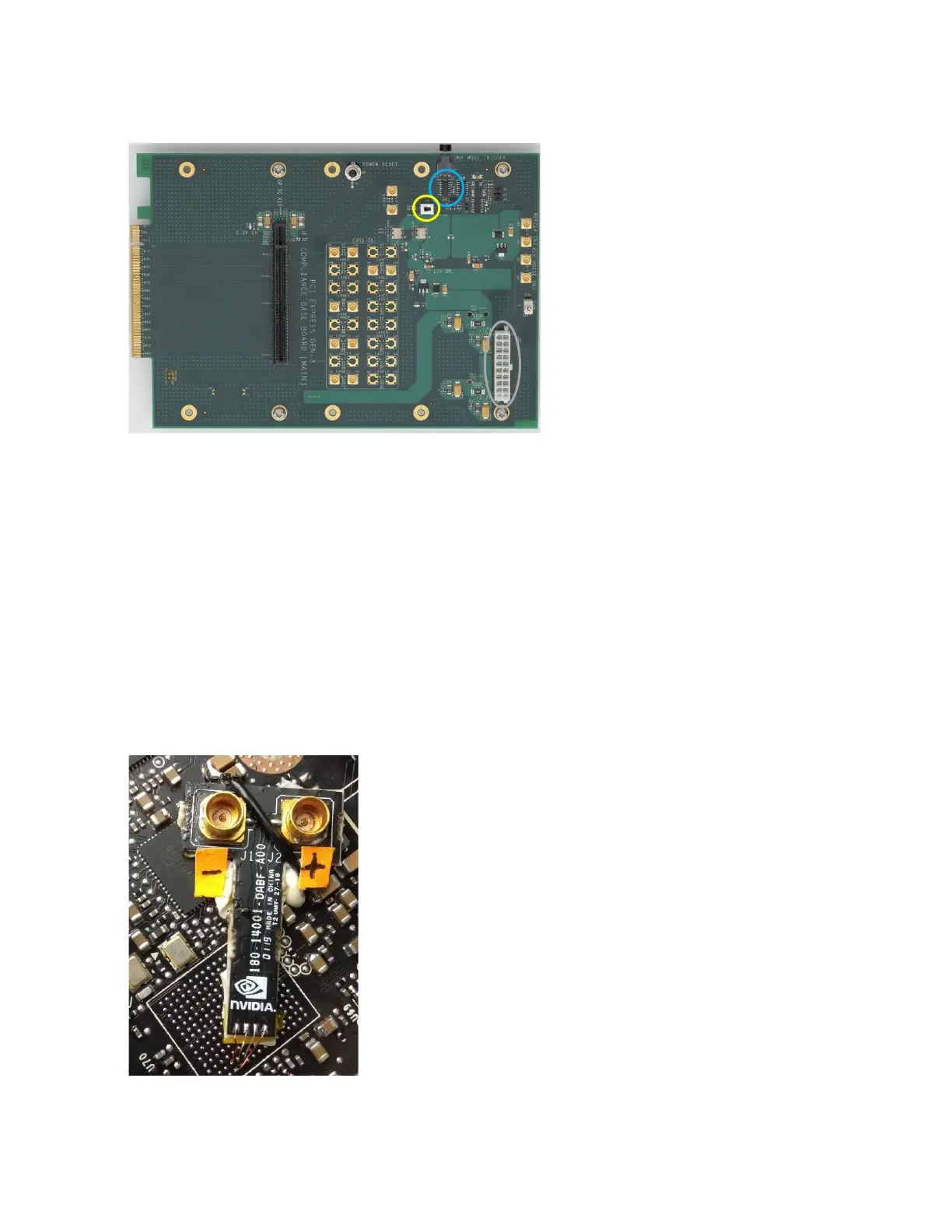
Breakout Boards
NVIDIA uses a proprietary purpose-built breakout board for differential measurement to tap
into the solder pads of the devices taken off the board. It may also be used to inject the 100
MHz and 1 ms trigger pulse on Rx lanes to a DUT. Customers are requested to create or
purchase an equivalent solution or use probe solder tips. The breakout board is a good
example of how to provide connectivity into the DUT.
When using a breakout board, use a breakout channel S-Parameter file used to de-embed the
breakout channel when necessary. When using the S-Parameter file, the scope must be
capable of convoluting real-time measurement with S-Parameters.
Figure 3. SMA Differential Breakout Board

 Loading...


