Do you have a question about the Nvidia Jetson AGX Xavier Series and is the answer not in the manual?
Lists and defines abbreviations used in the document.
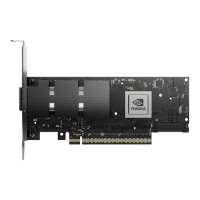
Describes the pinout and orientation of the 699-pin connector.
Details spacing requirements between module and carrier boards.
Provides recommendations for standoff heights for module mounting.
Outlines the procedure for installing and removing the module.
Details the internal power subsystem allocation for the module.
Describes the power-on sequencing requirements for system startup.
Explains the main system power supply input for SYS_VIN_HV.
Details the various power-on features and methods for the module.
Covers the requirements and considerations for power discharge circuitry.
Describes the power and voltage monitoring capabilities.
Explains the low power states supported by the module.
Explains the conventions used for naming signals in the document.
Describes the format used for specifying signal routing guidelines.
Outlines the conventions used for signal routing.
Provides an overview of routing rules for high-speed interfaces.
Offers general guidelines for PCB routing to minimize crosstalk.
Covers USB 2.0 and USB 3.1 port implementations and guidelines.
Details the PCI Express lanes and their configurations.
Describes the UFS interface and its design guidelines.
Covers DisplayPort and embedded DisplayPort interfaces and guidelines.
Details the HDMI interface support and connection examples.
Explains the MIPI CSI interfaces and their configurations.
Covers the SLVS-EC interface for cameras.
Details the SD card interface, connections, and routing requirements.
Provides signal routing requirements for the I2S interface.
Outlines signal routing requirements for the DMIC interface.
Details the I2C controllers and their mapping.
Covers the SPI interfaces and their pin descriptions.
Details the UART interfaces and their pin descriptions.
Covers the CAN interfaces and their pin descriptions.
Explains the USB recovery mode for flashing and debugging.
Shows the connections for JTAG and debug UART interfaces.
Describes the strapping pins for system configuration.
Details the requirements for supporting boundary scan test mode.
Outlines connections for the safety MCU on JAXi variants.
Explains MPIO pad behavior when associated power rails are enabled/disabled.
Describes the use of Schmitt triggers on MPIO pins for noise immunity.
Details pins that are pulled or driven during the power-on sequence.
Provides maximum MPIO pad output drive current specifications.
Lists MPIO pins that can be left unconnected if unused.
Identifies unused SFIO interface pins for potential use.
Provides guidelines for via count, placement, and types.
Discusses the importance of proper via connections for effectiveness.
Covers trace length, impedance, and layer stack-up requirements.
Details the reference design stack-up definitions and their impact.
Provides a primer on basic board-level transmission line theory.
Describes microstrip and stripline transmission line types.
Explains key driver equations for signal integrity.
Covers receiver concepts for optimum signal integrity.
Discusses reference plane identification for signal integrity.
Defines maximum trace delay and breakout delay.
Explains delay differences within and between differential pairs.
Defines trace impedance, spacing, and microstrip vs. stripline.
Covers ground reference return vias and proximity.
Provides techniques to minimize USB SS de-sense issues.
| GPU | 512-core Volta GPU with Tensor Cores |
|---|---|
| CPU | 8-core ARM v8.2 64-bit CPU, 8MB L2 + 4MB L3 |
| Memory | 32GB 256-Bit LPDDR4x | 137GB/s |
| Storage | 32GB eMMC 5.1 |
| DL Accelerator | 2x NVDLA Engines |
| Vision Accelerator | 7-way VLIW Vision Processor |
| Dimensions | 105 mm x 105 mm |
| AI Performance | 32 TOPS (INT8) |
| Connectivity | 10/100/1000 BASE-T Ethernet |
| PCIe | 16x PCIe Gen4 |
| USB | USB 3.1, USB 2.0 |
| Power | 10W / 15W / 30W |
| Display | eDP |