USB, PCIe, and UFS
Jetson AGX Xavier Series Product DG-09840-001_v2.5 | 56
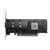
Void all layers of golden finger
area under the pad 5.7 mils
larger than the pad size is
recommended.
Keep critical PCIe traces such as PEX_TX/RX, TERMP etc. away from other signal traces or unrelated power traces/areas or
power supply components
Table 7-15. PCIe Signal Connections Module I/F Configured as Endpoint
PCIe Interface #C5 (Up to x8)
OUT
Design Guideline for
Differential Transmit Data Pairs: Connect to TX_P/N pins of
PCIe connector or
pin of PCIe device through AC
Design Guideline for
value) if device on main
Differential Receive Data Pairs: Connect to RX_P/N pins of
PCIe connector or
pin of PCIe device through AC caps.
Differential Reference Clock Output: Unused when
interface #C5 is used as Endpoint.
47KΩ pullup on module
to VDDIO_AO_3V3.
PEX Clock Request for PEX_CLK5: Connect to CLKREQ pin
on device/connector.
module to
PEX Reset: Connect to PERST pin on device/connector.
Differential Reference Clock Pair for NVHS0_SLVS
(Controller #5) interface. Connect 100MHz differential
clock source to the REFCLK pins when the PCIe interface
on NVHS pins is configured as Endpoint.
47KΩ pullup to
VDDIO_AO_3V3
on
PEX Wake: Unused for interfaces configured as Endpoint
Note: Check the “Supported USB 3.1 PEX and UFS Interface Mapping” tables earlier in this section for PCIe IF mapping
options.
Table 7-16. Recommended PCIe Observation Test Points for Initial Boards
Test Points Recommended Location
One for each of the PCIe TX_+/– output lines used. Near PCIe device. Connector pins may serve as test points
if accessible.
One for each of the PCIe RX_+/– input lines used. Near Jetson AGX Xavier connector.

 Loading...