Power
Jetson AGX Xavier Series Product DG-09840-001_v2.5 | 18
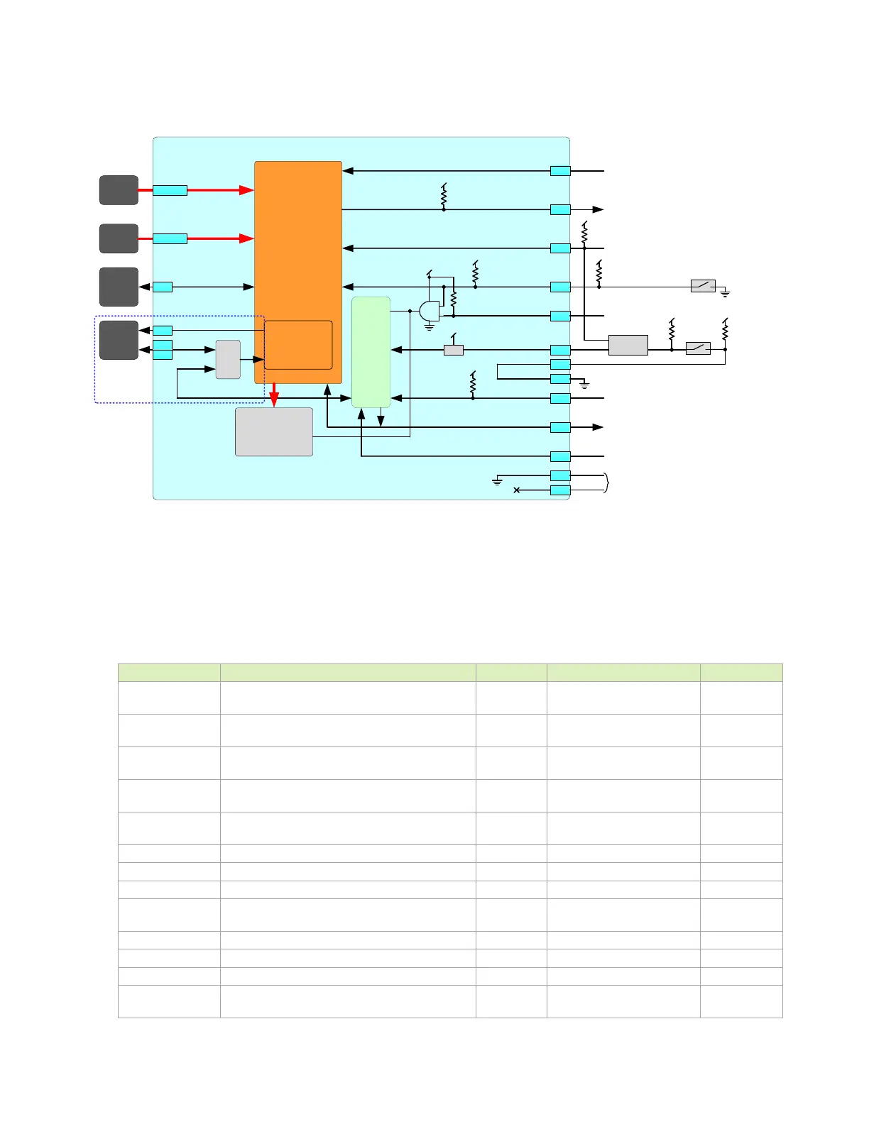
Figure 5-1. Power Block Diagram
Jetson AGX Xavier
9V-20V
Supply
L53
Memo ry/
Peripheral s
LPDDR4x,
eMMC
Power
Subsystem
5V/3.3V Pre
-Regs
PMU Switchers/
LDOs
CPU/GPU/Core/
CV Regs
Ext. LDOs
Load Switches
SoC
VCC_RTC
SYS_VIN_HV
L60
To carrier board power
subsystem. When active, carrier
boa rd can be gin powering on.
System reset to/from
carrier board
Optional
Battery
Back-up
1 . 8V
5V
Supply
SYS_VIN_MV
VDDIN_PWR_BAD_N
CARRIER_POWER_ON
MODULE_POWER_ON
SYS_RESET_N
PERIPHERAL_RESET_N
POWER_BTN_N
PRSNT1
PRSNT0
STANDBY_REQ_N
STANDBY_ACK_N
SYSTEM_OC_N
MID0
MID1
From carrier board VIN loss
detection circuit. When active,
all ows m odule to powe r on.
PO WER
RESE T
L55
L54
L62
J60
L58
L11
L61
A 61
From carrier board VIN loss
det ec tion, USB C PD p ower
path circuitry.
LVL
Powe r-on
circuitry
Optional:
Res ets only
SoC & eMMC.
1 . 8V
Optional system overcurrent
indicator from carrier board.
Signa l from module tha t it is
entering standby (SC7) mode.
Optional signal from carrier
board to request system to
enter standby (SC7) mode.
PU
3 . 3V
PU
5 . 0V
PU
1 . 8V
PU
1 . 8V
PU
1 . 8V
L63
A3
PU
3 . 3V
PU
Al wa ys ON
3 . 3V
Mult iple
Mult iple
Voltage
Monitors
L44
Safety
MCU
VM_I2C
L45
Mux
VM_INT_N
L47
JAXi Only
PWR_I2C
K40
H40
Module ID pins
5.1 Supply Allocation
Table 5-2 describes the power subsystem allocation for Jetson AGX Xavier.
Table 5-2. Internal Power Subsystem Allocation
Power Rails Usage (V) Power Supply Source
VDD_CPU SoC CPU rail Variable
NCP81276 and FDMF5833
(x2)
SYS_VIN_HV
VDD_GPU SoC GPU rail Variable
NCP81276 and FDMF5833
(x2)
SYS_VIN_HV
VDD_CORE (SOC) SoC Core rail Variable
NCP81276 and FDMF5833
(x2)
SYS_VIN_HV
VDD_CV SoC CV rail Variable
NCP81276 and FDMF5833
(x2)
SYS_VIN_HV
VDDIO_SYS_1V0
SoC AVDDIO_HDMI_DP[3:0], PEX_DVDD,
NVHS0_DVDD rails
1.0 PMIC Switcher SD0 SYS_VIN_MV
VDDIO_SYS_1V8HS See Note 1 1.8 PMIC Switcher SD1 SYS_VIN_MV
VDDIO_SYS_1V8LS See Note 2 1.8 PMIC Switcher SD2 SYS_VIN_MV
SoC AVDD_CSI and VDDIO_UFS rails (See note 3)
EN_VDD_1V0
Enable for FETs gating discharge of
VDDIO_SYS_1V0 rail (See note 3)
na PMIC LDO8 SYS_VIN_MV
VDDIO_AO_1V8 See Note 4 1.8 PMIC Switcher SD3 SYS_VIN_MV
DDR_AP_1V1 SoC VDDIO_DDRx rail 1.1 PMIC Switcher SD4 SYS_VIN_MV
VDD_RTC SoC RTC rail Variable PMIC LDO0 SYS_VIN_MV
DDR_VDD2_
1V1_EN
See Note 5 Na PMIC LDO1 SYS_VIN_MV

 Loading...