Power
Jetson AGX Xavier Series Product DG-09840-001_v2.5 | 31
Figure 5-13. VIN Loss Detection Circuit
TPS3808G01
SENSEVCC
R ST *
TP
GND
CT
MR*
5V_AO
VDDIN_PWR_BAD_N
RB5 21 S30 T1G
VDD_SRC
47.5kΩ, 1%
1nF
0.1uF
10nF
47.5kΩ, 1%
2. 49 kΩ, 1%
10 0k Ω, 1%
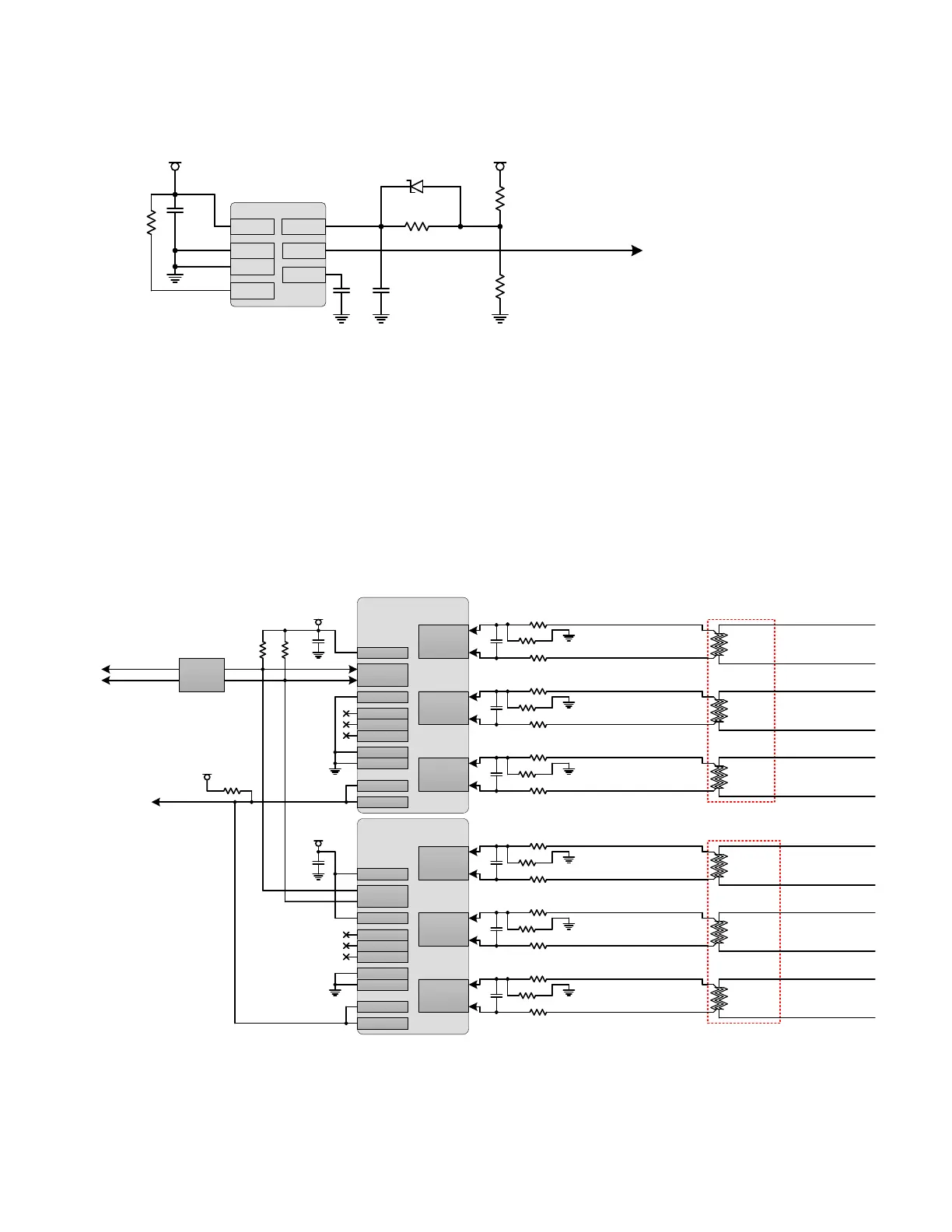
5.6.2 Power Monitor
Power monitors are provided on Jetson AGX Xavier. These monitor the VDD_GPU, VDD_CPU,
VDD_SOC (Core), VDD_CV, VDD_DDRQ, and SYS_VIN_MV Supplies. The monitors will toggle a WARN
(Warning) or CRIT (Critical) output, depending on the power “seen” at the sense resistors and
the thresholds set for each supply. This output is connected to the SOC_GPIO7 pin. The I2C
address for the top power monitor (GPU/CPU/SOC) is 7’H40, and for the bottom power monitor
(CV, VDDRQ, SYS_VIN_MV) is 7’H41).
Figure 5-14. Power Monitor
Sense
Resistors
I2C_GP2_ DAT
I2C_GP2_ CLK
INA3221AQRGVRQ1
Power Monitor
GPU_INA_P
0.005Ω, 1%
0805
0.1uF
GPU_INA_M
VIN_SYS_5V0
GPU Supply Monitor
CPU Supply Monitor
SOC Supply Monitor
CPU_INA_P
0.005Ω, 1%
0805
CPU_INA_M
SOC_INA_P
0.005Ω, 1%
0805
SOC_INA_M
20Ω
20Ω
20Ω
20Ω
20Ω
20Ω
VIN1 P
VIN1 N
WARN
CRIT
VS
AO
PV
TC
VPU
GND
SCL
SDA
PAD
VIN2 P
VIN2 N
VIN3 P
VIN3 N
SoC
SOC_GPIO7
SYS_VIN_HV
SYS_VIN_HV
VDD_SYS_CPU_IN
(CPU supply input)
VDD_SYS_GPU_IN
(GPU supply input)
VDD_SYS_SOC_IN
(SOC supply input)
SYS_VIN_HV
1uF
1uF
1uF
Sense
Resistors
INA3221AQRGVRQ1
Power Monitor
CV_INA_P
0.005Ω, 1%
0805
0.1uF
CV_INA_M
VIN_SYS_5V0
CV Supply Monitor
VDDRQ Supply Monitor
System 5V Supply Monitor
VDDRQ_INA_P
0.005Ω, 1%
0805
VDDRQ_INA_N
SYS5V_P
0.005Ω, 1%
0805
SYS5V_N
20Ω
20Ω
20Ω
20Ω
20Ω
20Ω
VIN1 P
VIN1 N
VS
AO
PV
TC
VPU
GND
SCL
SDA
PAD
VIN2 P
VIN2 N
VIN3 P
VIN3 N
SYS_VIN_HV
SYS_VIN_HV
VIN_SYS_DDRQ_IN
(DDRQ supply input)
VDD_SYS_CV_IN
(CV supply input)
VDD_SYS_5V0
(SYS_VIN_MV input)
SYS_VIN_MV
1uF
1uF
1uF
100kΩ
VDDIO_AO_1V8
VMON
Level
Shif te r
10kΩ
10kΩ
665kΩ
665kΩ
665kΩ
665kΩ
665kΩ
665kΩ
WARN
CRIT

 Loading...