Do you have a question about the Onkyo A-933 and is the answer not in the manual?
Instructions for replacing fuses, emphasizing using identical types.
Steps to initialize the unit by pressing specific buttons and disconnecting power.
Specifies default settings for power, tone controls, and volume before shipping.
Printed circuit board layout for the U01 Power Amplifier, component side.
Printed circuit board layout for the U01 Power Amplifier, soldering side.
Printed circuit board layout for U02 Pre-Amplifier, NAAF-8499 & NAAF-8500, side A.
Printed circuit board layout for U02 Pre-Amplifier, NAAF-8499 & NAAF-8500, side B.
Printed circuit board layout for U04 Volume PC Board, NAETC-8501 & NAETC-8502, side A.
Printed circuit board layout for U04 Volume PC Board, NAETC-8501 & NAETC-8502, side B.
Printed circuit board layout for U06 Headphone Jack PC Board, NAETC-8503, side A.
Printed circuit board layout for U06 Headphone Jack PC Board, NAETC-8503, side B.
Printed circuit board layout for U08 Microprocessor PC Board, NADG-8505, component side.
Printed circuit board layout for U08 Microprocessor PC Board, NADG-8505, soldering side.
Printed circuit board layout for U09 Power Supply PC Board, NAPS-8506, component side.
Printed circuit board layout for U09 Power Supply PC Board, NAPS-8506, soldering side.
Printed circuit board layout for U10 Outlet PC Board, NAPS-8507, component side.
Printed circuit board layout for U11 Power Switch PC Board, NASW-8508, component side.
Printed circuit board layout for U13 Switch PC Board, NAETC-8510, component side.
Printed circuit board layout for U13 Switch PC Board, NAETC-8510, soldering side.
Block diagram for the Q204 NJU7313AM Analog Function Switch IC.
Detailed terminal descriptions for the Q204 NJU7313AM IC.
Terminal descriptions for the Q701 Microprocessor, part 1.
Terminal descriptions for the Q701 Microprocessor, part 2.
Conditions requiring DC offset adjustment on the power amplifier PC board.
Step-by-step guide to adjust DC offset on the power amplifier PC board.
Comprehensive list of parts for the U01 Power Amplifier PC Board.
Comprehensive list of parts for the U02 Pre-Amplifier PC Board.
Comprehensive list of parts for the U04 Volume PC Board.
Comprehensive list of parts for the U06 Headphone Jack PC Board.
| Frequency range | 10 - 60000 Hz |
|---|---|
| Signal-to-Noise Ratio (SNR) | 100 dB |
| Total Harmonic Distortion (THD) | 0.08 % |
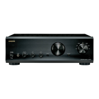
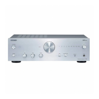
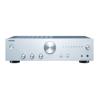
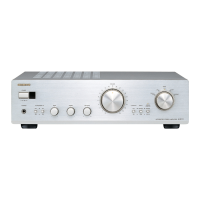
| Product color | Black |
| Dimensions (WxDxH) | 275 x 103 x 328 mm |
| Power requirements | AC 220-240 V, 50 Hz |
| Power consumption (standby) | 0.9 W |
| Power consumption (typical) | 100 W |
| Weight | 7500 g |
|---|