IC BLOCK DIAGRAMS AND TERMINAL DESCRIPTIONS-15
Q421 : CS42518 (8-Ch Codec with S/PDIF Receiver)-2/4
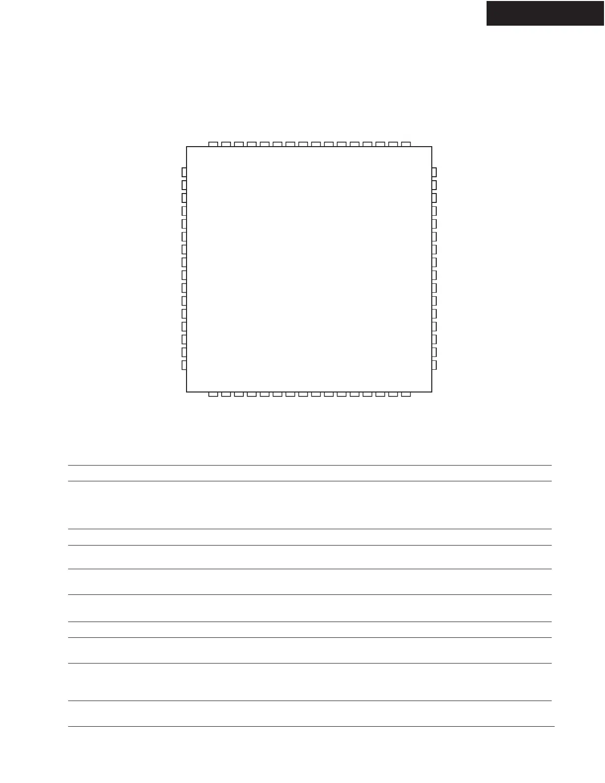
PIN LAYOUT
TERMINAL DESCRIPTION
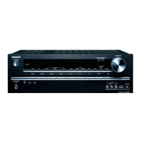
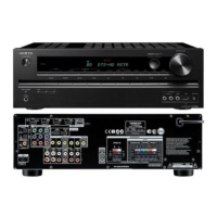
TX-SR503/503E/8350
Pin Name # Pin Description
CX_SDIN1
CX_SDIN2
CX_SDIN3
CX_SDIN4
1
64
63
62
Codec Serial Audio Data Input (Input) - Input for two's complement serial audio data.
CX_SCLK CODEC Serial Clock (Input/Output) - Serial clock for the CODEC serial audio interface
CX_LRCK
VD
DGND
VLC
SCL/CCLK
SDA/CDOUT
AD1/CDIN
CODEC Left Right Clock (Input/ Output) - Determines which channel, Left or Right, is currently active on
the CODEC serial audio data line.
Digital Power (Input) - Positive power supply for the digital section.
Digital Ground (Input) - Ground reference. Should be connected to digital ground.
Control Port Power (Input) - Determines the required signal level for the control port.
Serial Control Port Clock (Input) - Serial clock for the serial control port. Requires an external pull-up
resistor to the logic interface voltage in I2C mode as shown in the Typical Connection Diagram.
Serial Control Data (Input/Output) - SDA is a data I/O line in IC mode and requires an external pull-up
resistor to the logic interface voltage, as shown in the Typical connection Diagram. CDOUT is the output
data line for the control port interface in SPI mode.
Address Bit 1 (I2C)/Serial Control Data (SPI) (Input) - AD1 a chip address pin in I2C mode; CDIN is
the input data line for control port interface in SPI mode.
2
3
4
51
5
52
6
7
8
9
RXP1/GP01
RXP1/GP01
RXP1/GP01
RXP1/GP01
RXP1/GP01
RXP1/GP01
RXP1/GP01
VARX
AGND
LPFLT
MUTEC
AOUTA1-
AOUTA1+
AOUTB1+
AOUTB1-
AOUTA2-
CX_SDIN2
CX_SDIN3
CX_SDIN4
SAI_SCLK
SAI_LRCK
OMCK
ADCIN1
ADCIN2
CX_SDOUT
RMCK
SAI_SDOUT
VLS
DGND
VD
TXP
RXPO
CX_SDIN1
CX_SCLK
CX_LRCK
VD
DGND
VLC
SCL/CCLK
SDA/CDOUT
AD1/CDIN
AD0/CS
INT
RST
AINR-
AINR+
AINL+
AINL-
VQ
FILT+
REFGND
AOUTB4-
AOUTB4+
AOUTA4+
AOUTA4-
VA
AGND
AOUTB3-
AOUTB3+
AOUTA3+
AOUTA3-
AOUTB2-
AOUTB2+
AOUTA2+
48
47
46
45
44
43
42
41
40
39
38
37
36
35
34
33
1
2
3
4
5
6
7
8
9
10
11
12
13
14
15
16
64
63
62
61
60
59
58
57
56
55
54
53
52
51
50
49
17
18
19
20
21
22
23
24
25
26
27
28
29
30
31
32
CS42518
 Loading...