IC BLOCK DIAGRAMS AND TERMINAL DESCRIPTIONS-24
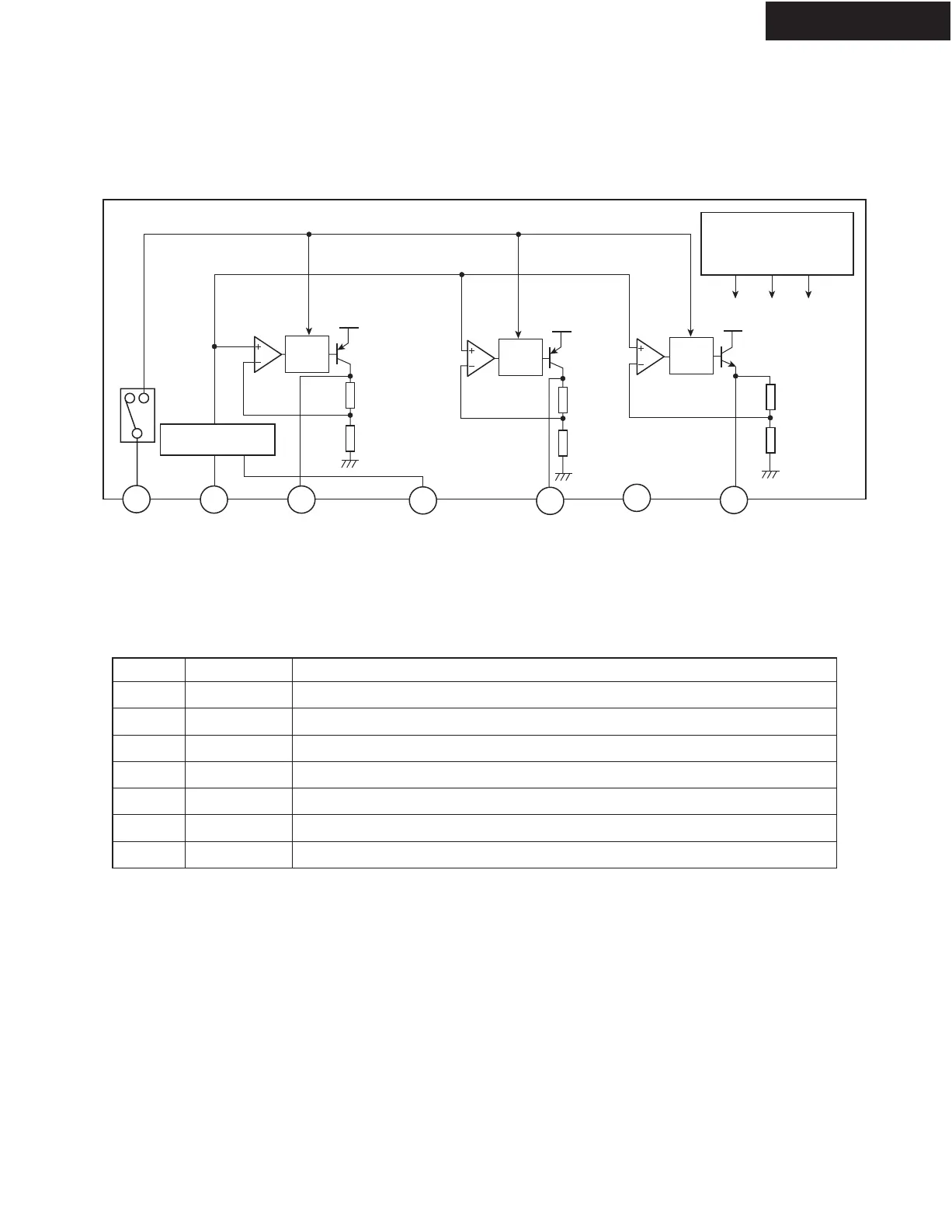
Q5640: AN34060A (3 Output Voltage Regulator)
BLOCK DIAGRAM
TERMINAL DESCRIPTION
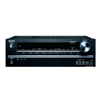
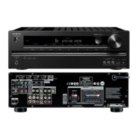
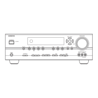
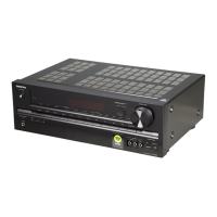
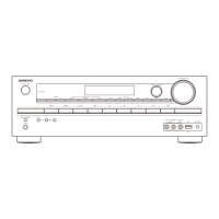
TX-SR503/503E/8350
Description
MODE 1
REG 1
VCC
GND
REG 2
VCC
REG 3
Function
WHEN MODE 1 pin is 5V, REG 1 output is "H".
WHEN MODE 1 pin is "H", REG 1 output is 5.0V (Io1(peak) = 300mA min).
Connected to Power supply
Connected to IC substrate
WHEN MODE 1 pin is "H", REG 2 output is 3.3V (Io2(peak) = 200mA min).
Connected to Power supply
WHEN MODE 1 pin is "H", REG 3 output is 2.5V (I
o3(peak) = 600mA min).
Pin No.
1
2
3
4
5
6
7
Pre
Drive
VCC
Output
Pre
Drive
Peak Current
Protection &
Thermal Protection
Reference Voltage
1
3
6
2
7
4
5
VCC
VCC
Pre
Drive
 Loading...