TX-L55/LR552
IC BLOCK DIAGRAMS AND DESCRIPTIONS
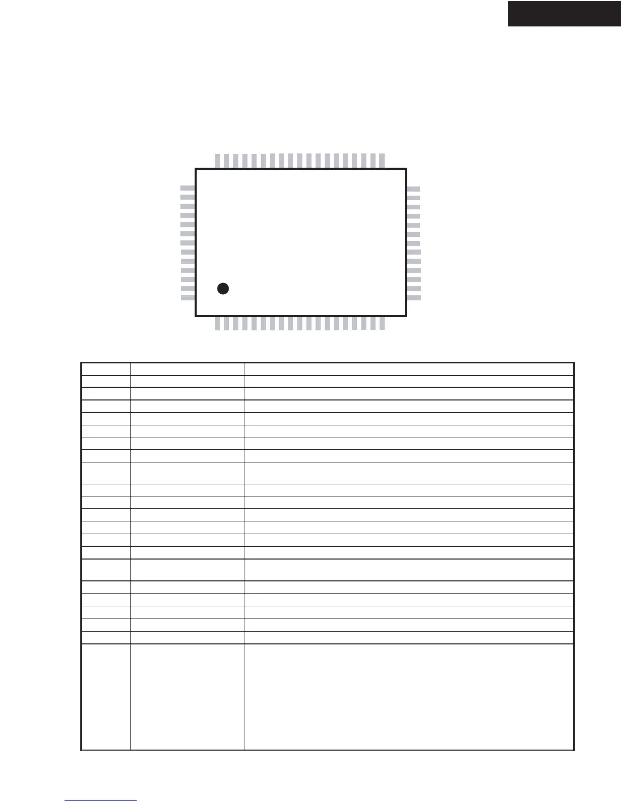
TC2150(Digital Power Amplifier Driver)
Pin Connection
Y2B
NC
NC
OCD2
TSS
NC
OCD1
V5
AGND
NC
NC
NC
Y2
NC
Y1
Y1B
NC
NC
NC
NC
OCS2LP
NC
NC
NC
OCS1LN
OCS1LP
NC
NC
52
2658
57
55
54
56
53
64-pin LQFP
(Top View)
27
28
29
NC
OCS2LN
VBOOT2
VBOOT1
32
31
30
NC
NC
NC
SMPSO
SW-FB
64
63
61
60
62
59
NC
NC
NC
NC
NC
20
21
22
23
NC
NC
25
24
1
14131110 12
98765432 191716 1815
45 44 42 4143
40 39 38
37
36 35 34 33
51 50 48 4749
46
OCS1HN
NC
LO2
VN10
VNN
VN10
LO1
LO1COM
NC
HO1COM
HO1
NC
OCS1HP
LO2COM
OCS2HN
NC
HO2
HO2COM
OCS2HP
NC
Pin Description
Pin Function Description
5 AGND Analog
ground.
6 V5 5V power supply
input.
7 OCD1
Over-current threshold output (Channel 1)
9 TSS This a test pin for the TP2350B. Th
is pin should be left floating.
10 OCD2 Over-current th
reshold output (Channel 2)
13,17 Y2, Y1 Non-inverted sw
itching modulator inputs
14,16 Y2B, Y1B Inverted sw
itching modulator inputs
27,57 VBOOT2, VBOOT1 Bootstrapped voltage to supply drive to gate of high-side FET
(Channel 2 & 1)
30,31 OCS2LP, OCS2LN Over Current Sense inputs, Channel 2 low-
side
33,34 OCS2HP, OCS2HN Over Current
Sense inputs, Channel 2 high-side
36,48 HO2, HO1 High side gate
drive output (Channel 2 & 1)
37,47 HO2COM, HO1COM Kelvin connection to source of high-side transistor (Channel 2 & 1)
39,45 LO2COM, LO1COM Kelvin connection to source of low-
side transistor (Channel 2 & 1)
40,44 LO2, LO1 Low side gate
drive output (Channel 2 & 1)
41,43 VN10 “Floating” supply input for the FET drive circuitry. This voltage must be stable
and referenced to VNN.
42 VNN Negative supply
voltage.
50,51 OCS1HN, OCS1HP Over Current
Sense inputs, Channel 1 high-side
53,54 OCS1LN ,OCS1LP Over Current Sense inputs, Channel 1 low-
side
59 SW-FB Feedback for regulating switching power supply
output for VN10
60 SMPSO Switching power supply
output for VN10
1,2,3,4,8,
11,12,15,
18,19,20,
21,22,23,
24,25,26,
28,29,32,
35,38,46,
49,52,55,
56,58,61,
62,63,64
NC Not connected (bonded) internally. Leave these pins floating.

 Loading...