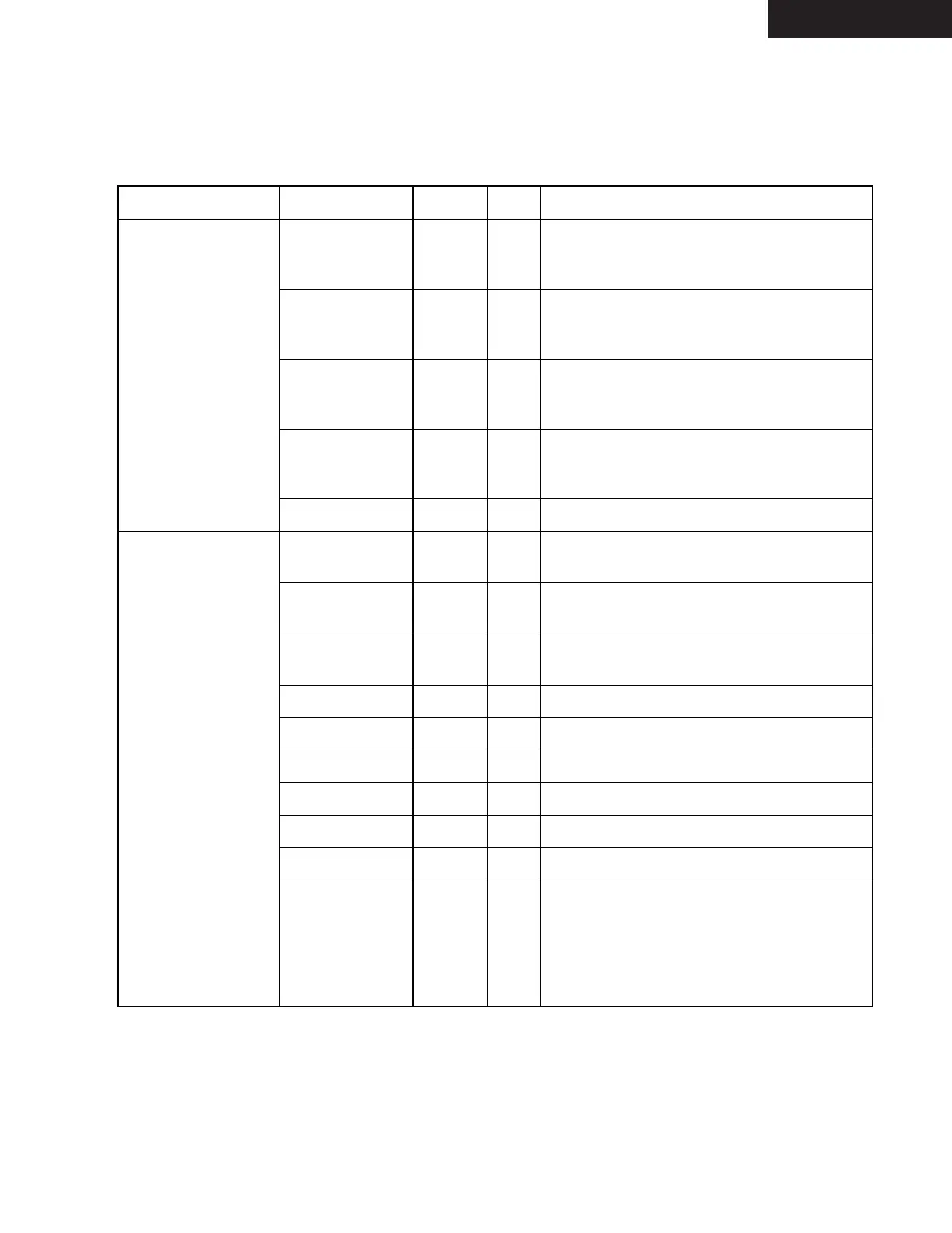
IC BLOCK DIAGRAMS AND TERMINAL DESCRIPTIONS -31
Q8001 : SII504 (I/P Video Converter)
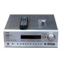
TX-SR674/674E/8467
TERMINAL DESCRIPTION (1/5)
Signal Group
Signal Name
Notes
Type
Description
Video Input VidInData[9:2] 5V In Multiplexed Video Input Data (ITU-R BT.656,
8-bit & H/V syncs formats); Y (luma) Video
Input Data (16-bit & H/V syncs format).
VidInData[19:12] 5V/PD In Chroma Video Input Data (16-bit & H/V syncs
(HostData[15:8]) format only). See Host Interface pin list for
pin functions when not used for video input.
VS 5V/PD In Vertical Sync input (8/16-bit & H/V syncs
(HostData[7]) format only). See Host Interface pin list for
pin function when not used for video input.
HS 5V/PD In Horizontal Sync input (8/16-bit & H/V syncs
(HostData[6]) format only). See Host Interface pin list for
pin function when not used for video input.
VidInClk 5V In
Video Input Clock, 27.0 MHz
Video Output Red_Cr[9:0] Out Red Data (RGB output mode);
Cr Data (YCrCb output mode)
Green_Y[9:0] Out Green Data (RGB output mode);
Y Data (YCrCb output mode)
Blue_Cb[9:0] Out Blue Data (RGB output mode);
Cb Data (YCrCb output mode)
/HSync Out
Horizontal Sync
/VSync Out
Vertical Sync
/CSync Out
Composite Sync
/CBlank Out
Composite Blank
LCDPwrEn Out
LCD Power Enable
VidOutClk Out
Video Output Clock, 36, 27 or 24 MHz
Clk48M 5V InOut 48 MHz Clock. Normally, this pin is a no-
connect, outputting an internal PLL-generated
48.0 MHz clock and receiving that same clock
through its input buffer. To bypass the PLL,
set /BypPLLClk48M = 0, and supply a 48.0
MHz clock to the Clk48M pin.