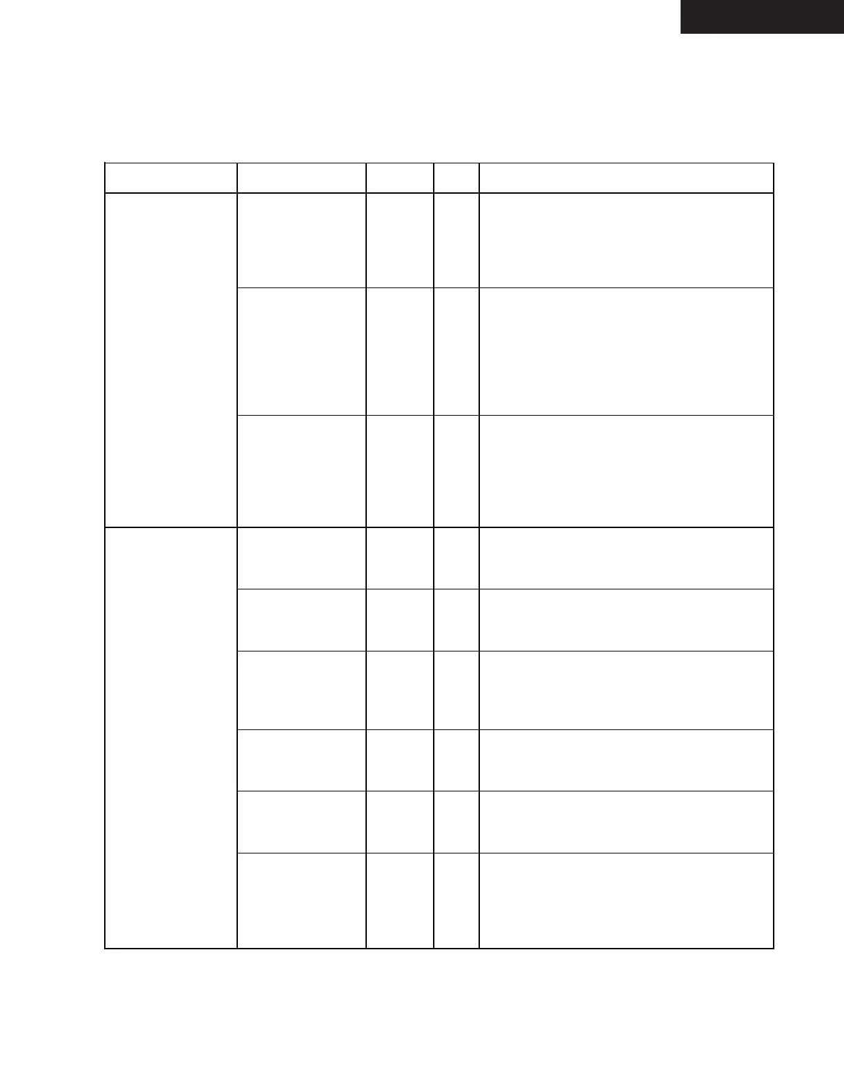
IC BLOCK DIAGRAMS AND TERMINAL DESCRIPTIONS -32
Q8001 : SII504 (I/P Video Converter)
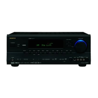
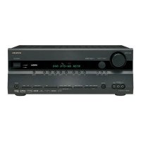
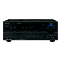
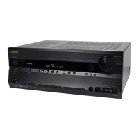
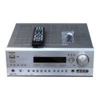
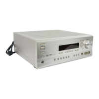
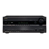
TX-SR674/674E/8467
Signal Group
Signal Name
Notes
Type
Description
Video Output /BypPLLClk48M PU In Bypass PLL for Clk48M. Normally, this pin is
(continued) a no-connect, and the internal pullup ensures
that the PLL is enabled. To bypass the PLL,
set /BypPLLClk48M = 0, and supply a 48.0
MHz clock to the Clk48M pin.
Clk54_72M 5V InOut 54 or 72 MHz Clock. Normally, this pin is a
no-connect, outputting an internal PLL-
generated 54.0 MHz or 72.0 MHz clock and
receiving that same clock through its input
buffer. To bypass the PLL, set
/BypPLLClk54_72M = 0, and supply a 54.0
or 72.0 MHz clock to the Clk54_72M pin.
-
/BypPLLClk54_72M 5V/PU In Bypass PLL for Clk54_72M. Normally, this
pin is a no-connect, and the internal pullup
ensures that the PLL is enabled. To bypass
the PLL, set /BypPLLClk54_72M = 0, and
supply a 54.0 MHz or 72.0 MHz clock to the
Clk54_72M pin.
Audio/Video SDIn 5V/PD In Serial Digital Audio Input Data. See Audio/
Synchronization Video Synchronization section of Functional
Description for audio formats supported.
WSIn 5V/PD In Serial Digital Audio Input Word Select. See
Audio/Video Synchronization section for audio
formats supported.
SCKIn 5V/PD In Serial Digital Audio Input Clock. Frequency
range of clock is 1.411 to 6.144 MHz. See
Audio/Video Synchronization section for
audio formats supported.
SDOut Out Serial Digital Audio Output Data. Audio
output follows audio input, with a delay equal
to that of the video processing pipeline.
WSOut Out Serial Digital Audio Output Word Select.
Audio output follows audio input, with a delay
equal to that of the video processing pipeline.
SCKOut
5V/PD In Serial Digital Audio Output Clock. Same
frequency as SCKIn. SDOut and WSOut are
generated from SCKOut. See Audio/Video
Synchronization section for more details on
on audio clocking.
TERMINAL DESCRIPTION (2/5)